SNVSC61A August   2022  – December 2022 LP5891-Q1

PRODUCTION DATA  

  1. Features
  2. Applications
  3. Description
  4. Revision History
  5. Description (continued)
  6. Pin Configuration and Functions
  7. Specifications
    1. 7.1 Absolute Maximum Ratings
    2. 7.2 ESD Ratings
    3. 7.3 Recommended Operating Conditions
    4. 7.4 Thermal Information
    5. 7.5 Electrical Characteristics
    6. 7.6 Timing Requirements
    7. 7.7 Switching Characteristics
    8. 7.8 Typical Characteristics
  8. Detailed Description
    1. 8.1 Overview
    2. 8.2 Functional Block Diagram
    3. 8.3 Feature Description
      1. 8.3.1 Independent and Stackable Mode
        1. 8.3.1.1 Independent Mode
        2. 8.3.1.2 Stackable Mode
      2. 8.3.2 Current Setting
        1. 8.3.2.1 Brightness Control (BC) Function
        2. 8.3.2.2 Color Brightness Control (CC) Function
        3. 8.3.2.3 Choosing BC/CC for a Different Application
      3. 8.3.3 Frequency Multiplier
      4. 8.3.4 Line Transitioning Sequence
      5. 8.3.5 Protections and Diagnostics
        1. 8.3.5.1 Thermal Shutdown Protection
        2. 8.3.5.2 IREF Resistor Short Protection
        3. 8.3.5.3 LED Open Load Detection and Removal
          1. 8.3.5.3.1 LED Open Detection
          2. 8.3.5.3.2 Read LED Open Information
          3. 8.3.5.3.3 LED Open Caterpillar Removal
        4. 8.3.5.4 LED Short and Weak Short Circuitry Detection and Removal
          1. 8.3.5.4.1 LED Short/Weak Short Detection
          2. 8.3.5.4.2 Read LED Short Information
          3. 8.3.5.4.3 LSD Caterpillar Removal
    4. 8.4 Device Functional Modes
    5. 8.5 Continuous Clock Series Interface
      1. 8.5.1 Data Validity
      2. 8.5.2 CCSI Frame Format
      3. 8.5.3 Write Command
        1. 8.5.3.1 Chip Index Write Command
        2. 8.5.3.2 VSYNC Write Command
        3. 8.5.3.3 MPSM Write Command
        4. 8.5.3.4 Standby Clear and Enable Command
        5. 8.5.3.5 Soft_Reset Command
        6. 8.5.3.6 Data Write Command
      4. 8.5.4 Read Command
    6. 8.6 PWM Grayscale Control
      1. 8.6.1 Grayscale Data Storage and Display
        1. 8.6.1.1 Memory Structure Overview
        2. 8.6.1.2 Details of Memory Bank
        3. 8.6.1.3 Write a Frame Data into Memory Bank
      2. 8.6.2 PWM Control for Display
    7. 8.7 Register Maps
      1. 8.7.1  FC0
      2. 8.7.2  FC1
      3. 8.7.3  FC2
      4. 8.7.4  FC3
      5. 8.7.5  FC4
      6. 8.7.6  FC14
      7. 8.7.7  FC15
      8. 8.7.8  FC16
      9. 8.7.9  FC17
      10. 8.7.10 FC18
      11. 8.7.11 FC19
      12. 8.7.12 FC20
      13. 8.7.13 FC21
  9. Application and Implementation
    1. 9.1 Application Information
    2. 9.2 Typical Application
      1. 9.2.1 Design Requirements
        1. 9.2.1.1 System Structure
        2. 9.2.1.2 SCLK Frequency
        3. 9.2.1.3 Internal GCLK Frequency
        4. 9.2.1.4 Line Switch Time
        5. 9.2.1.5 Blank Time Removal
        6. 9.2.1.6 BC and CC
      2. 9.2.2 Detailed Design Procedure
        1. 9.2.2.1 Chip Index Command
        2. 9.2.2.2 FC Registers Settings
        3. 9.2.2.3 Grayscale Data Write
        4. 9.2.2.4 VSYNC Command
        5. 9.2.2.5 LED Open, Short Read
      3. 9.2.3 Application Curves
    3. 9.3 Power Supply Recommendations
    4. 9.4 Layout
      1. 9.4.1 Layout Guidelines
      2. 9.4.2 Layout Example
  10. 10Device and Documentation Support
    1. 10.1 Documentation Support
      1. 10.1.1 Related Documentation
    2. 10.2 Receiving Notification of Documentation Updates
    3. 10.3 Support Resources
    4. 10.4 Trademarks
    5. 10.5 Electrostatic Discharge Caution
    6. 10.6 Glossary
  11. 11Mechanical, Packaging, and Orderable Information

Package Options

Mechanical Data (Package|Pins)
Thermal pad, mechanical data (Package|Pins)
Orderable Information

Memory Structure Overview

The LP5891-Q1 implements a display memory unit to achieve high refresh rate and high contrast ratio in an LED display products. The internal display memory unit is divided into two BANKs: BANK A and BANK B. During the normal operation, one BANK is selected to display the data of current frame, another is used to restore the data of next frame. The BANK switcher is controlled by the BANK_SEL bit, which is an internal flag register bit.

After power on, BANK_SEL is initialized to 0, and BANK A is selected to restore the data of next frame. Meanwhile, the data in BANK B is read out for display. When one frame has elapsed, the controller sends the vertical synchronization (VSYNC) command to start the next frame, the BANK_SEL bit value is toggled and the selection of the two BANKs reverses. Repeat this operation until all the frame images are displayed.

With this method, the LP5891-Q1 device can display the current frame image at a very high refresh rate. See Figure 8-26 for more details about the BANK-selection exchange operation.
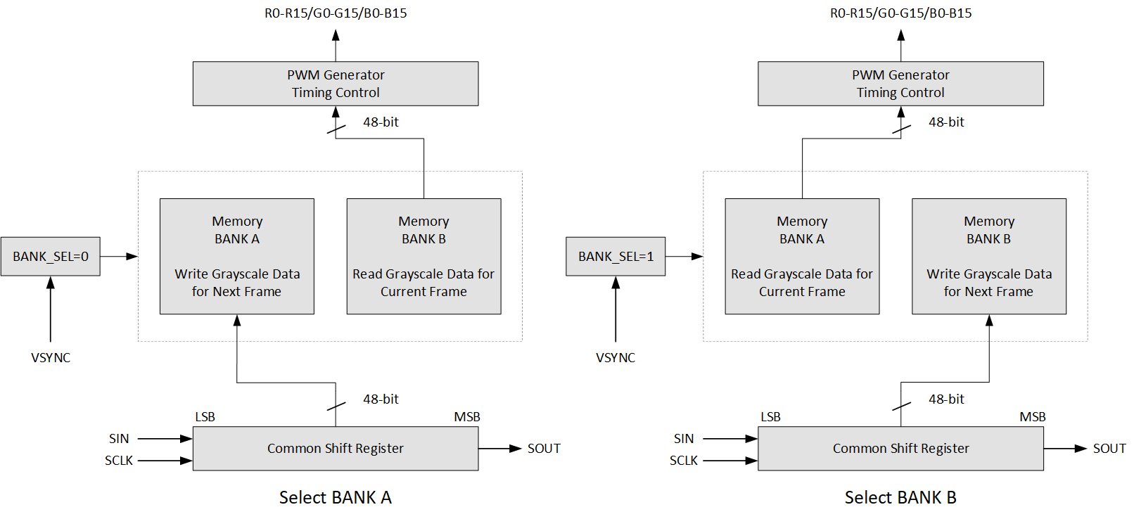
GUID-20220224-SS0I-T9S5-J0SD-ZTKJBWKQZ85V-low.gif Figure 8-26 Bank Selection Exchange Operation