SNVSAW2B April   2017  – December 2018 LP87524B-Q1 , LP87524J-Q1 , LP87524P-Q1

PRODUCTION DATA.  

  1. Features
  2. Applications
    1.     Simplified Schematic
  3. Description
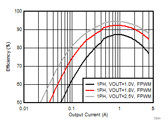
    1.     Efficiency vs Output Current
  4. Revision History
  5. Pin Configuration and Functions
    1.     Pin Functions
  6. Specifications
    1. 6.1 Absolute Maximum Ratings
    2. 6.2 ESD Ratings
    3. 6.3 Recommended Operating Conditions
    4. 6.4 Thermal Information
    5. 6.5 Electrical Characteristics
    6. 6.6 I2C Serial Bus Timing Requirements
    7. 6.7 Typical Characteristics
  7. Detailed Description
    1. 7.1 Overview
    2. 7.2 Functional Block Diagram
    3. 7.3 Feature Descriptions
      1. 7.3.1 DC-DC Converters
        1. 7.3.1.1 Overview
        2. 7.3.1.2 Transition Between PWM and PFM Modes
        3. 7.3.1.3 Buck Converter Load-Current Measurement
        4. 7.3.1.4 Spread-Spectrum Mode
      2. 7.3.2 Sync Clock Functionality
      3. 7.3.3 Power-Up
      4. 7.3.4 Regulator Control
        1. 7.3.4.1 Enabling and Disabling Regulators
        2. 7.3.4.2 Changing Output Voltage
      5. 7.3.5 Enable and Disable Sequences
      6. 7.3.6 Device Reset Scenarios
      7. 7.3.7 Diagnostics and Protection Features
        1. 7.3.7.1 Power-Good Information (PGOOD pin)
        2. 7.3.7.2 Warnings for Diagnostics (Interrupt)
          1. 7.3.7.2.1 Output Power Limit
          2. 7.3.7.2.2 Thermal Warning
        3. 7.3.7.3 Protection (Regulator Disable)
          1. 7.3.7.3.1 Short-Circuit and Overload Protection
          2. 7.3.7.3.2 Overvoltage Protection
          3. 7.3.7.3.3 Thermal Shutdown
        4. 7.3.7.4 Fault (Power Down)
          1. 7.3.7.4.1 Undervoltage Lockout
      8. 7.3.8 GPIO Signal Operation
      9. 7.3.9 Digital Signal Filtering
    4. 7.4 Device Functional Modes
      1. 7.4.1 Modes of Operation
    5. 7.5 Programming
      1. 7.5.1 I2C-Compatible Interface
        1. 7.5.1.1 Data Validity
        2. 7.5.1.2 Start and Stop Conditions
        3. 7.5.1.3 Transferring Data
        4. 7.5.1.4 I2C-Compatible Chip Address
        5. 7.5.1.5 Auto-Increment Feature
    6. 7.6 Register Maps
      1. 7.6.1 Register Descriptions
        1. 7.6.1.1  OTP_REV
          1. Table 10. OTP_REV Register Field Descriptions
        2. 7.6.1.2  BUCK0_CTRL1
          1. Table 11. BUCK0_CTRL1 Register Field Descriptions
        3. 7.6.1.3  BUCK1_CTRL1
          1. Table 12. BUCK1_CTRL1 Register Field Descriptions
        4. 7.6.1.4  BUCK2_CTRL1
          1. Table 13. BUCK2_CTRL1 Register Field Descriptions
        5. 7.6.1.5  BUCK3_CTRL1
          1. Table 14. BUCK3_CTRL1 Register Field Descriptions
        6. 7.6.1.6  BUCK0_VOUT
          1. Table 15. BUCK0_VOUT Register Field Descriptions
        7. 7.6.1.7  BUCK0_FLOOR_VOUT
          1. Table 16. BUCK0_FLOOR_VOUT Register Field Descriptions
        8. 7.6.1.8  BUCK1_VOUT
          1. Table 17. BUCK1_VOUT Register Field Descriptions
        9. 7.6.1.9  BUCK1_FLOOR_VOUT
          1. Table 18. BUCK1_FLOOR_VOUT Register Field Descriptions
        10. 7.6.1.10 BUCK2_VOUT
          1. Table 19. BUCK2_VOUT Register Field Descriptions
        11. 7.6.1.11 BUCK2_FLOOR_VOUT
          1. Table 20. BUCK2_FLOOR_VOUT Register Field Descriptions
        12. 7.6.1.12 BUCK3_VOUT
          1. Table 21. BUCK3_VOUT Register Field Descriptions
        13. 7.6.1.13 BUCK3_FLOOR_VOUT
          1. Table 22. BUCK3_FLOOR_VOUT Register Field Descriptions
        14. 7.6.1.14 BUCK0_DELAY
          1. Table 23. BUCK0_DELAY Register Field Descriptions
        15. 7.6.1.15 BUCK1_DELAY
          1. Table 24. BUCK1_DELAY Register Field Descriptions
        16. 7.6.1.16 BUCK2_DELAY
          1. Table 25. BUCK2_DELAY Register Field Descriptions
        17. 7.6.1.17 BUCK3_DELAY
          1. Table 26. BUCK3_DELAY Register Field Descriptions
        18. 7.6.1.18 GPIO2_DELAY
          1. Table 27. GPIO2_DELAY Register Field Descriptions
        19. 7.6.1.19 GPIO3_DELAY
          1. Table 28. GPIO3_DELAY Register Field Descriptions
        20. 7.6.1.20 RESET
          1. Table 29. RESET Register Field Descriptions
        21. 7.6.1.21 CONFIG
          1. Table 30. CONFIG Register Field Descriptions
        22. 7.6.1.22 INT_TOP1
          1. Table 31. INT_TOP1 Register Field Descriptions
        23. 7.6.1.23 INT_TOP2
          1. Table 32. INT_TOP2 Register Field Descriptions
        24. 7.6.1.24 INT_BUCK_0_1
          1. Table 33. INT_BUCK_0_1 Register Field Descriptions
        25. 7.6.1.25 INT_BUCK_2_3
          1. Table 34. INT_BUCK_2_3 Register Field Descriptions
        26. 7.6.1.26 TOP_STAT
          1. Table 35. TOP_STAT Register Field Descriptions
        27. 7.6.1.27 BUCK_0_1_STAT
          1. Table 36. BUCK_0_1_STAT Register Field Descriptions
        28. 7.6.1.28 BUCK_2_3_STAT
          1. Table 37. BUCK_2_3_STAT Register Field Descriptions
        29. 7.6.1.29 TOP_MASK1
          1. Table 38. TOP_MASK1 Register Field Descriptions
        30. 7.6.1.30 TOP_MASK2
          1. Table 39. TOP_MASK2 Register Field Descriptions
        31. 7.6.1.31 BUCK_0_1_MASK
          1. Table 40. BUCK_0_1_MASK Register Field Descriptions
        32. 7.6.1.32 BUCK_2_3_MASK
          1. Table 41. BUCK_2_3_MASK Register Field Descriptions
        33. 7.6.1.33 SEL_I_LOAD
          1. Table 42. SEL_I_LOAD Register Field Descriptions
        34. 7.6.1.34 I_LOAD_2
          1. Table 43. I_LOAD_2 Register Field Descriptions
        35. 7.6.1.35 I_LOAD_1
          1. Table 44. I_LOAD_1 Register Field Descriptions
        36. 7.6.1.36 PGOOD_CTRL1
          1. Table 45. PGOOD_CTRL1 Register Field Descriptions
        37. 7.6.1.37 PGOOD_CTRL2
          1. Table 46. PGOOD_CTRL2 Register Field Descriptions
        38. 7.6.1.38 PGOOD_FLT
          1. Table 47. PGOOD_FLT Register Field Descriptions
        39. 7.6.1.39 PLL_CTRL
          1. Table 48. PLL_CTRL Register Field Descriptions
        40. 7.6.1.40 PIN_FUNCTION
          1. Table 49. PIN_FUNCTION Register Field Descriptions
        41. 7.6.1.41 GPIO_CONFIG
          1. Table 50. GPIO_CONFIG Register Field Descriptions
        42. 7.6.1.42 GPIO_IN
          1. Table 51. GPIO_IN Register Field Descriptions
        43. 7.6.1.43 GPIO_OUT
          1. Table 52. GPIO_OUT Register Field Descriptions
  8. Application and Implementation
    1. 8.1 Application Information
    2. 8.2 Typical Application
      1. 8.2.1 Design Requirements
        1. 8.2.1.1 Inductor Selection
        2. 8.2.1.2 Input Capacitor Selection
        3. 8.2.1.3 Output Capacitor Selection
        4. 8.2.1.4 Snubber Components
        5. 8.2.1.5 Supply Filtering Components
      2. 8.2.2 Current Limit vs. Maximum Output Current
      3. 8.2.3 Detailed Design Procedure
      4. 8.2.4 Application Curves
  9. Power Supply Recommendations
  10. 10Layout
    1. 10.1 Layout Guidelines
    2. 10.2 Layout Example
  11. 11Device and Documentation Support
    1. 11.1 Device Support
      1. 11.1.1 Third-Party Products Disclaimer
    2. 11.2 Related Links
    3. 11.3 Receiving Notification of Documentation Updates
    4. 11.4 Community Resources
    5. 11.5 Trademarks
    6. 11.6 Electrostatic Discharge Caution
    7. 11.7 Glossary
  12. 12Mechanical, Packaging, and Orderable Information
  13. 12Mechanical, Packaging, and Orderable Information

Package Options

Refer to the PDF data sheet for device specific package drawings

Mechanical Data (Package|Pins)
  • RNF|26
Thermal pad, mechanical data (Package|Pins)
Orderable Information

Application Curves

Measurements are done using typical application set up with connections shown in Figure 65 (snubber components included when VIN > 4 V). Graphs may not reflect the OTP default settings. Unless otherwise specified: VIN = 3.7 V, VOUT = 1 V, V(NRST) = 1.8 V, TA = 25°C, ƒSW = 4 MHz, L = 0.47 µH (TOKO DFE252012PD-R47M), COUT = 22 µF / phase, and CPOL = 22 µF / phase. Measurements are done using connections in the Typical Application.
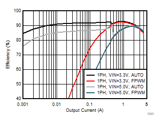
LP87524B-Q1 LP87524J-Q1 LP87524P-Q1 D923_LP8756.gif
VOUT = 1.8 V
Figure 67. Efficiency in PFM/PWM Mode
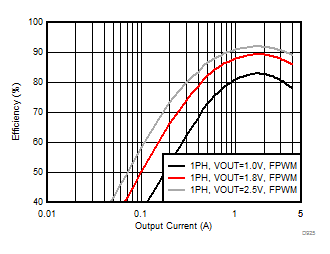
LP87524B-Q1 LP87524J-Q1 LP87524P-Q1 D925_LP8756.gif
VIN = 5 V
Figure 69. Efficiency in Forced-PWM Mode
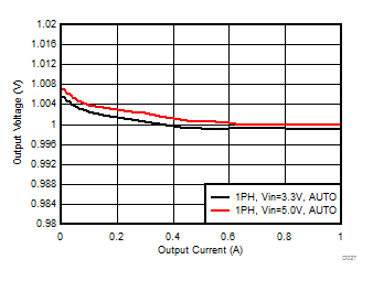
LP87524B-Q1 LP87524J-Q1 LP87524P-Q1 D027_LP8756.gifFigure 71. Output Voltage vs Load Current in PFM/PWM Mode
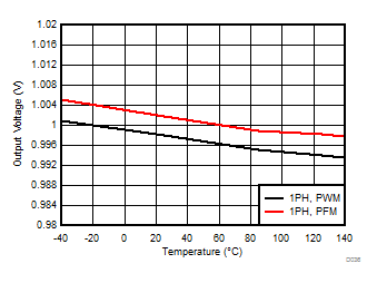
LP87524B-Q1 LP87524J-Q1 LP87524P-Q1 D036_LP8756.gif
Load = 1 A (PWM) and 0.1 A (PFM)
Figure 73. Output Voltage vs Temperature
LP87524B-Q1 LP87524J-Q1 LP87524P-Q1 D906_LP8756.gif
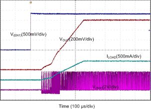
RLOAD = 1 Ω
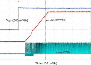
Figure 75. Start-Up With EN1, Forced PWM
(1-Phase Output)
LP87524B-Q1 LP87524J-Q1 LP87524P-Q1 D999_LP8756.gif
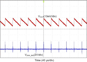
IOUT = 10 mA
Figure 77. Output Voltage Ripple, PFM Mode
(1-Phase Output)
LP87524B-Q1 LP87524J-Q1 LP87524P-Q1 D300_SNVSAW2.gif
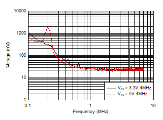
VOUT = 1 V No load RBW/VBW = 10 Hz
Figure 79. Output Voltage Ripple Spectrum, Forced-PWM Mode. COUT = 22 µF, ferrite BLM18KG121TH1D, CPOL = 10 µF + 0.22 µF.
LP87524B-Q1 LP87524J-Q1 LP87524P-Q1 D996_LP8756.gif
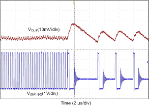
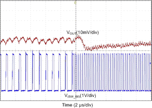
Figure 81. Transient from PWM-to-PFM Mode
(1-Phase Output)
LP87524B-Q1 LP87524J-Q1 LP87524P-Q1 D994_LP8756.gif
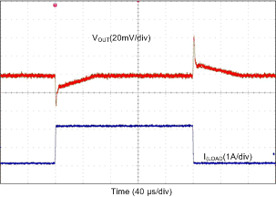
IOUT = 0.1 A → 2 A → 0.1 A TR = TF = 1 µs
Figure 83. Transient Load Step Response, Forced-PWM Mode (1-Phase Output)
LP87524B-Q1 LP87524J-Q1 LP87524P-Q1 D364_LP8752.gif
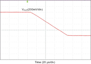
Figure 85. VOUT Transition from 1.4 V to 0.6 V
LP87524B-Q1 LP87524J-Q1 LP87524P-Q1 D924_LP8756.gif
VIN = 3.3 V
Figure 68. Efficiency in Forced-PWM Mode
LP87524B-Q1 LP87524J-Q1 LP87524P-Q1 D026_LP8756.gif
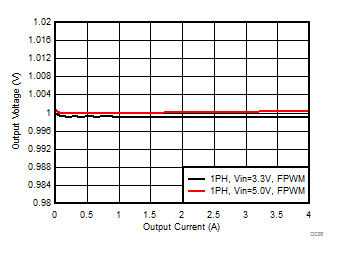
Figure 70. Output Voltage vs Load Current in Forced-PWM Mode
LP87524B-Q1 LP87524J-Q1 LP87524P-Q1 D028_LP8756.gif
VOUT = 1 V Load = 1 A
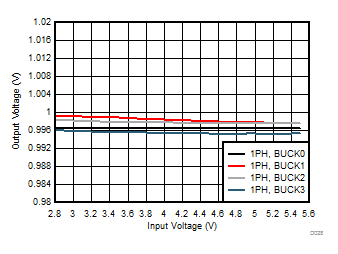
Figure 72. Output Voltage vs Input Voltage in PWM Mode
LP87524B-Q1 LP87524J-Q1 LP87524P-Q1 D905_LP8756.gif
IOUT = 0 A
Figure 74. Start-Up With EN1, Forced PWM
LP87524B-Q1 LP87524J-Q1 LP87524P-Q1 D907_LP8756.gif
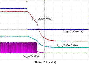
RLOAD = 1 Ω
Figure 76. Shutdown With EN1, Forced PWM
(1-Phase Output)
LP87524B-Q1 LP87524J-Q1 LP87524P-Q1 D998_LP8756.gif
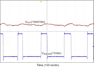
IOUT = 200 mA
Figure 78. Output Voltage Ripple, Forced-PWM Mode
(1-Phase Output)
LP87524B-Q1 LP87524J-Q1 LP87524P-Q1 D997_LP8756.gif
Figure 80. Transient from PFM-to-PWM Mode
(1-Phase Output)
LP87524B-Q1 LP87524J-Q1 LP87524P-Q1 D995_LP8756.gif
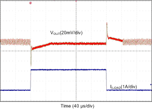
IOUT = 0.1 A → 2 A → 0.1 A TR = TF = 1 µs
Figure 82. Transient Load Step Response, AUTO Mode
(1-Phase Output)
LP87524B-Q1 LP87524J-Q1 LP87524P-Q1 D365_LP8752.gif
Figure 84. VOUT Transition from 0.6 V to 1.4 V
LP87524B-Q1 LP87524J-Q1 LP87524P-Q1 D098_LP8756.gif
Figure 86. Start-up With Short on Output (1-Phase Output)