SNVS861A February 2014 – August 2014 LP8754
PRODUCTION DATA.
- 1 Features
- 2 Applications
- 3 Description
- 4 Revision History
- 5 Pin Configuration and Functions
-
6 Specifications
- 6.1 Absolute Maximum Ratings
- 6.2 Handling Ratings
- 6.3 Recommended Operating Conditions
- 6.4 Thermal Information
- 6.5 General Electrical Characteristics
- 6.6 6-Phase Buck Electrical Characteristics
- 6.7 6-Phase Buck System Characteristics
- 6.8 Protection Features Characteristics
- 6.9 I2C Serial Bus Timing Parameters
- 6.10 Typical Characteristics
-
7 Detailed Description
- 7.1 Overview
- 7.2 Functional Block Diagram
- 7.3 Features Descriptions
- 7.4 Device Functional Modes
- 7.5 Programming
- 7.6
Register Maps
- 7.6.1 Register Descriptions
- 7.6.2 VSET_B0
- 7.6.3 FPWM
- 7.6.4 BUCK0_CTRL
- 7.6.5 BUCK1_CTRL
- 7.6.6 BUCK2_CTRL
- 7.6.7 BUCK3_CTRL
- 7.6.8 BUCK4_CTRL
- 7.6.9 BUCK5_CTRL
- 7.6.10 FLAGS_0
- 7.6.11 FLAGS_1
- 7.6.12 INT_MASK_0
- 7.6.13 GENERAL
- 7.6.14 RESET
- 7.6.15 DELAY_BUCK0
- 7.6.16 CHIP_ID
- 7.6.17 PFM_LEV_B0
- 7.6.18 PHASE_LEV_B0
- 7.6.19 SEL_I_LOAD
- 7.6.20 LOAD_CURR
- 7.6.21 INT_MASK_2
- 8 Application and Implementation
- 9 Power Supply Recommendations
- 10Layout
- 11Device and Documentation Support
- 12Mechanical, Packaging, and Orderable Information
Package Options
Mechanical Data (Package|Pins)
- YFQ|49
Thermal pad, mechanical data (Package|Pins)
Orderable Information
1 Features
- Six High-Efficiency Step-Down DC/DC Converter Cores:
- Max Output Current 10 A
- Cores Bundled to a 6-Phase Converter
- Load Current Reporting
- Programmable Overcurrent Protection (OCP)
- Auto PWM/PFM and Forced-PWM Operations and Automatic Low Power-Mode Setting
- Automatic Phase Adding/Shedding
- Remote Differential Feedback Voltage Sensing
- Output Voltage Ramp Control
- VOUT Range = 0.6 V to 1.67 V
- I2C-Compatible Interface which Supports Standard (100 kHz), Fast (400 kHz), and High-Speed (3.4 MHz) Modes
- Four Selectable I2C Addresses
- Interrupt Function with Programmable Masking
- Output Short-Circuit and Input Overvoltage Protection (OVP)
- Spread Spectrum and Phase Control for EMI Reduction
- Overtemperature Protection (OTP)
- Undervoltage Lock-out (UVLO)
2 Applications
- Smart Phones, eBooks and Tablets
- GSM, GPRS, EDGE, LTE, CDMA and WCDMA Handsets
- Gaming Devices
3 Description
The LP8754 is designed to meet the power management requirements of the latest applications processors in mobile phones and similar portable applications. The device contains six step-down DC/DC converter cores, which are bundled together in a 6-phase buck converter. The device is fully controlled by a Dynamic Voltage Scaling (DVS) interface or an I2C-compatible serial interface.
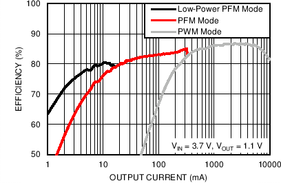
The automatic PWM/PFM operation together with the automatic phase adding/shedding maximizes efficiency over a wide output current range. The LP8754 supports remote differential voltage sensing to compensate IR drop between the regulator output and the point-of-load thus improving the accuracy of the output voltage.
The protection features include short-circuit protection, current limits, input OVP, UVLO, temperature warning, and shutdown functions. Several error flags are provided for status information of the IC. In addition, I2C read-back includes total load current and load current for each buck core: The LP8754 has the ability to sense current being delivered to the load without the addition of current sense resistors. During start-up, the device controls the output voltage slew rate to minimize overshoot and the inrush current.
Device Information(1)
| PART NUMBER | PACKAGE | BODY SIZE (MAX) |
|---|---|---|
| LP8754 | DSBGA (49) | 3.022 mm x 2.882 mm |
- For all available packages, see the orderable addendum at the end of the datasheet.
Efficiency vs. Load Current
4 Revision History
| DATE | REVISION | NOTES |
|---|---|---|
| August 2014 | Rev. A | Initial release to Web |