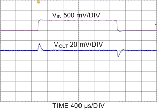
SNVSA06C March   2015  – August 2018 LP8758-B0

PRODUCTION DATA.  

  1. Features
  2. Applications
  3. Description
  4. Simplified Schematic
    1.     Efficiency vs Output Current (VIN = 3.7 V)
  5. Revision History
  6. Pin Configuration and Functions
    1.     Pin Functions
  7. Specifications
    1. 7.1 Absolute Maximum Ratings
    2. 7.2 ESD Ratings
    3. 7.3 Recommended Operating Conditions
    4. 7.4 Thermal Information
    5. 7.5 Electrical Characteristics
    6. 7.6 I2C Serial Bus Timing Parameter
    7. 7.7 Switching Characteristics
    8. 7.8 Typical Characteristics
  8. Detailed Description
    1. 8.1 Overview
      1. 8.1.1 Buck Information
        1. 8.1.1.1 Operating Modes
        2. 8.1.1.2 Features
        3. 8.1.1.3 Programmability
    2. 8.2 Functional Block Diagram
    3. 8.3 Feature Description
      1. 8.3.1 Multi-Phase DC-DC Converters
        1. 8.3.1.1 Overview
        2. 8.3.1.2 Multi-Phase Operation and Phase Adding/Shedding
        3. 8.3.1.3 Transition Between PWM and PFM Modes
        4. 8.3.1.4 Multi-Phase Switcher Configurations
        5. 8.3.1.5 Buck Converter Load Current Measurement
        6. 8.3.1.6 Spread-Spectrum Mode
      2. 8.3.2 Power-Up
      3. 8.3.3 Regulator Control
        1. 8.3.3.1 Enabling and Disabling Regulator
        2. 8.3.3.2 Changing Output Voltage
      4. 8.3.4 Device Reset Scenarios
      5. 8.3.5 Diagnosis and Protection Features
        1. 8.3.5.1 Warnings for Diagnosis (Interrupt)
          1. 8.3.5.1.1 Output Current Limit
          2. 8.3.5.1.2 Thermal Warning
        2. 8.3.5.2 Protection (Regulator Disable)
          1. 8.3.5.2.1 Short-Circuit and Overload Protection
          2. 8.3.5.2.2 Thermal Shutdown
        3. 8.3.5.3 Fault (Power Down)
          1. 8.3.5.3.1 Undervoltage Lockout
      6. 8.3.6 Digital Signal Filtering
    4. 8.4 Device Functional Modes
      1. 8.4.1 Modes of Operation
    5. 8.5 Programming
      1. 8.5.1 I2C-Compatible Interface
        1. 8.5.1.1 Data Validity
        2. 8.5.1.2 Start and Stop Conditions
        3. 8.5.1.3 Transferring Data
        4. 8.5.1.4 I2C-Compatible Chip Address
        5. 8.5.1.5 Auto Increment Feature
    6. 8.6 Register Maps
      1. 8.6.1 Register Descriptions
        1. 8.6.1.1  DEV_REV
        2. 8.6.1.2  OTP_REV
        3. 8.6.1.3  BUCK0_CTRL1
        4. 8.6.1.4  BUCK0_CTRL2
        5. 8.6.1.5  BUCK1_CTRL2
        6. 8.6.1.6  BUCK2_CTRL2
        7. 8.6.1.7  BUCK3_CTRL2
        8. 8.6.1.8  BUCK0_VOUT
        9. 8.6.1.9  BUCK0_FLOOR_VOUT
        10. 8.6.1.10 BUCK0_DELAY
        11. 8.6.1.11 RESET
        12. 8.6.1.12 CONFIG
        13. 8.6.1.13 INT_TOP
        14. 8.6.1.14 INT_BUCK_0_1
        15. 8.6.1.15 INT_BUCK_2_3
        16. 8.6.1.16 TOP_STAT
        17. 8.6.1.17 BUCK_0_1_STAT
        18. 8.6.1.18 BUCK_2_3_STAT
        19. 8.6.1.19 TOP_MASK
        20. 8.6.1.20 BUCK_0_1_MASK
        21. 8.6.1.21 BUCK_2_3_MASK
        22. 8.6.1.22 SEL_I_LOAD
        23. 8.6.1.23 I_LOAD_2
        24. 8.6.1.24 I_LOAD_1
  9. Application and Implementation
    1. 9.1 Application Information
    2. 9.2 Typical Application
      1. 9.2.1 Design Requirements
      2. 9.2.2 Detailed Design Procedure
        1. 9.2.2.1 Application Components
          1. 9.2.2.1.1 Inductor Selection
          2. 9.2.2.1.2 Input Capacitor Selection
          3. 9.2.2.1.3 Output Capacitor Selection
      3. 9.2.3 Application Curves
  10. 10Power Supply Recommendations
  11. 11Layout
    1. 11.1 Layout Guidelines
    2. 11.2 Layout Example
  12. 12Device and Documentation Support
    1. 12.1 Device Support
      1. 12.1.1 Third-Party Products Disclaimer
    2. 12.2 Documentation Support
      1. 12.2.1 Related Documentation
    3. 12.3 Receiving Notification of Documentation Updates
    4. 12.4 Community Resources
    5. 12.5 Trademarks
    6. 12.6 Electrostatic Discharge Caution
    7. 12.7 Glossary
  13. 13Mechanical, Packaging, and Orderable Information

Package Options

Mechanical Data (Package|Pins)
Thermal pad, mechanical data (Package|Pins)
Orderable Information

Application Curves

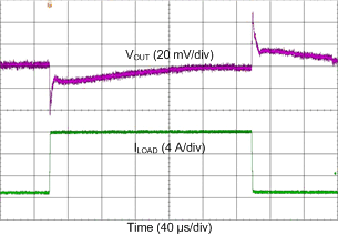
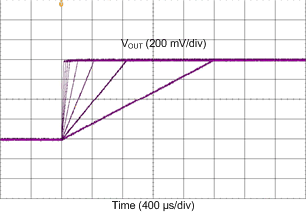
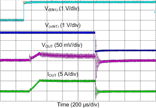
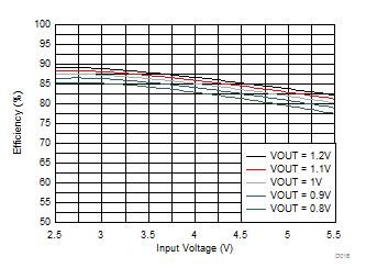
Unless otherwise specified: VIN = 3.7 V, VOUT = 1 V, V(NRST) = 1.8 V, TA = 25 °C, ƒSW = 3 MHz, L = 330 nH (TOKO DFE252010F-R33M), CPOL = 22 µF. Measurements done with connections in Figure 21.
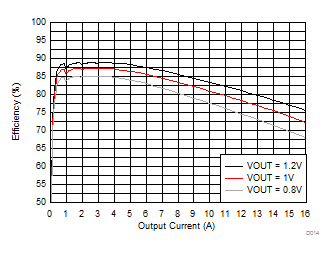
LP8758-B0 D014_snvsa06.gif
VIN = 3.7 V
Figure 22. Efficiency in Forced PWM Mode
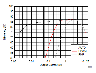
LP8758-B0 D002_snvsa06.gif
VIN = 3.7 V VOUT = 1 V
Figure 24. Efficiency in PFM, PWM and Forced Multi-Phase Mode
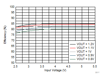
LP8758-B0 D017_snvsa06.gif
Load = 8 A
Figure 26. Efficiency vs Input Voltage
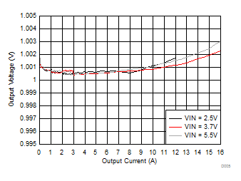
LP8758-B0 D005_snvsa06.gif
VOUT = 1 V
Figure 28. Output Voltage vs Load Current in Forced PWM Mode
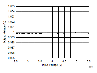
LP8758-B0 D044_snvsa06.gif
VOUT = 1 V Load = 1 A
Figure 30. Output Voltage vs Input Voltage in PWM Mode
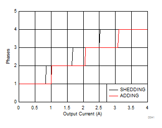
LP8758-B0 D041_snvsa06.gifFigure 32. Phase Adding and Shedding vs Load Current
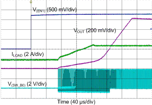
LP8758-B0 D021_startup_fpwm_3A.gif
Load = 3 A
Figure 34. Start-up with EN1, Forced PWM
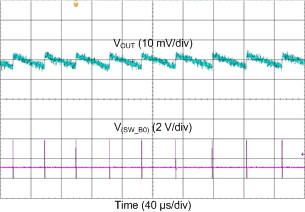
LP8758-B0 D034_pfm_ripple.gif
Load = 10 mA
Figure 36. Output Voltage Ripple, PFM Mode
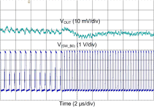
LP8758-B0 D023_pfm_to_pwm.gif
Figure 38. Transient from PFM-to-PWM Mode
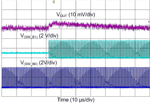
LP8758-B0 D028_phase_adding_1to2ph.gifFigure 40. Transient from 1-Phase to 2-Phase Operation
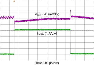
LP8758-B0 D025_load_transient_0A1to4A1_100ns_AUTO.gif
Load = 0.1 A → 4.1 A → 0.1 A TR = TF = 100 ns
Figure 42. Transient Load Step Response, AUTO Mode
LP8758-B0 D037_load_transient_1to12A_1us_fpwm.gif
Load = 1 A → 12 A → 1 A TR = TF = 1 µs
Figure 44. Transient Load Step Response, FPWM Mode
LP8758-B0 D026_slewrate.gif
Figure 46. VOUT Transition from 0.6 V to 1.4 V with Different Slew Rate Settings
LP8758-B0 D043_startup_with_short.gifFigure 48. Start-up with Short on Output
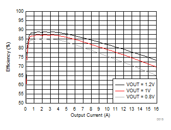
LP8758-B0 D015_snvsa06.gif
VIN = 3.7 V Inductor = TDK VLS252010HBX-R47M
Figure 23. Efficiency in Forced PWM Mode
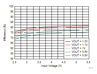
LP8758-B0 D016_snvsa06.gif
Load = 1 A
Figure 25. Efficiency vs Input Voltage
LP8758-B0 D018_snvsa06.gif
Load = 12 A
Figure 27. Efficiency vs Input Voltage
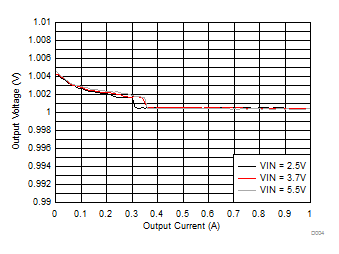
LP8758-B0 D004_snvsa06.gif
VOUT = 1 V
Figure 29. Output Voltage vs Load Current in PWM-PFM Mode
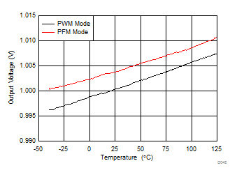
LP8758-B0 D045_SNVSA06.gif
VOUT = 1 V
Load = 3 A (PWM Mode) and 100 mA (PFM Mode)
Figure 31. Output Voltage vs Temperature
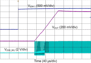
LP8758-B0 D020_startup_fpwm.gif
Load = 0 A
Figure 33. Start-up with EN1, Forced PWM
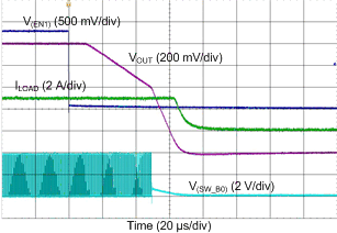
LP8758-B0 D022_shutdown_fpwm_3A.gif
Load = 3 A
Figure 35. Shutdown with EN1, Forced PWM
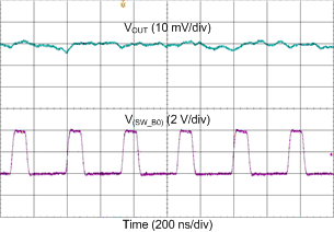
LP8758-B0 D035_pwm_ripple.gif
Load = 200 mA
Figure 37. Output Voltage Ripple, Forced PWM Mode
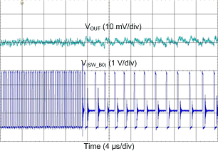
LP8758-B0 D024_pwm_to_pfm.gif
Figure 39. Transient from PWM-to-PFM Mode
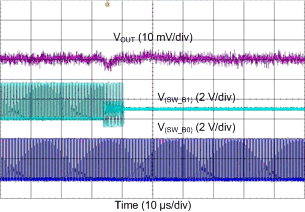
LP8758-B0 D033_phase_shedding_2to1ph.gifFigure 41. Transient from 2-Phase to 1-Phase Operation
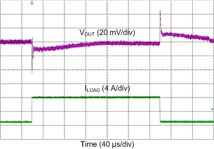
LP8758-B0 D036_load_transient_1to8A_400ns_fpwm.gif
Load = 1 A → 8 A → 1 A TR = TF = 400 ns
Figure 43. Transient Load Step Response, FPWM Mode
LP8758-B0 D027_line_transient_2V5to3V.gif
Load = 12 A TR = TF = 10 µs
VIN = 2.5 V → 3 V → 2.5 V
Figure 45. Transient Line Response
LP8758-B0 D042_slewrate_down.gif
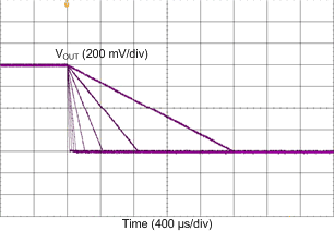
Figure 47. VOUT Transition from 1.4 V to 0.6 V with Different Slew Rate Settings