SNVSA06C March   2015  – August 2018 LP8758-B0

PRODUCTION DATA.  

  1. Features
  2. Applications
  3. Description
  4. Simplified Schematic
    1.     Efficiency vs Output Current (VIN = 3.7 V)
  5. Revision History
  6. Pin Configuration and Functions
    1.     Pin Functions
  7. Specifications
    1. 7.1 Absolute Maximum Ratings
    2. 7.2 ESD Ratings
    3. 7.3 Recommended Operating Conditions
    4. 7.4 Thermal Information
    5. 7.5 Electrical Characteristics
    6. 7.6 I2C Serial Bus Timing Parameter
    7. 7.7 Switching Characteristics
    8. 7.8 Typical Characteristics
  8. Detailed Description
    1. 8.1 Overview
      1. 8.1.1 Buck Information
        1. 8.1.1.1 Operating Modes
        2. 8.1.1.2 Features
        3. 8.1.1.3 Programmability
    2. 8.2 Functional Block Diagram
    3. 8.3 Feature Description
      1. 8.3.1 Multi-Phase DC-DC Converters
        1. 8.3.1.1 Overview
        2. 8.3.1.2 Multi-Phase Operation and Phase Adding/Shedding
        3. 8.3.1.3 Transition Between PWM and PFM Modes
        4. 8.3.1.4 Multi-Phase Switcher Configurations
        5. 8.3.1.5 Buck Converter Load Current Measurement
        6. 8.3.1.6 Spread-Spectrum Mode
      2. 8.3.2 Power-Up
      3. 8.3.3 Regulator Control
        1. 8.3.3.1 Enabling and Disabling Regulator
        2. 8.3.3.2 Changing Output Voltage
      4. 8.3.4 Device Reset Scenarios
      5. 8.3.5 Diagnosis and Protection Features
        1. 8.3.5.1 Warnings for Diagnosis (Interrupt)
          1. 8.3.5.1.1 Output Current Limit
          2. 8.3.5.1.2 Thermal Warning
        2. 8.3.5.2 Protection (Regulator Disable)
          1. 8.3.5.2.1 Short-Circuit and Overload Protection
          2. 8.3.5.2.2 Thermal Shutdown
        3. 8.3.5.3 Fault (Power Down)
          1. 8.3.5.3.1 Undervoltage Lockout
      6. 8.3.6 Digital Signal Filtering
    4. 8.4 Device Functional Modes
      1. 8.4.1 Modes of Operation
    5. 8.5 Programming
      1. 8.5.1 I2C-Compatible Interface
        1. 8.5.1.1 Data Validity
        2. 8.5.1.2 Start and Stop Conditions
        3. 8.5.1.3 Transferring Data
        4. 8.5.1.4 I2C-Compatible Chip Address
        5. 8.5.1.5 Auto Increment Feature
    6. 8.6 Register Maps
      1. 8.6.1 Register Descriptions
        1. 8.6.1.1  DEV_REV
        2. 8.6.1.2  OTP_REV
        3. 8.6.1.3  BUCK0_CTRL1
        4. 8.6.1.4  BUCK0_CTRL2
        5. 8.6.1.5  BUCK1_CTRL2
        6. 8.6.1.6  BUCK2_CTRL2
        7. 8.6.1.7  BUCK3_CTRL2
        8. 8.6.1.8  BUCK0_VOUT
        9. 8.6.1.9  BUCK0_FLOOR_VOUT
        10. 8.6.1.10 BUCK0_DELAY
        11. 8.6.1.11 RESET
        12. 8.6.1.12 CONFIG
        13. 8.6.1.13 INT_TOP
        14. 8.6.1.14 INT_BUCK_0_1
        15. 8.6.1.15 INT_BUCK_2_3
        16. 8.6.1.16 TOP_STAT
        17. 8.6.1.17 BUCK_0_1_STAT
        18. 8.6.1.18 BUCK_2_3_STAT
        19. 8.6.1.19 TOP_MASK
        20. 8.6.1.20 BUCK_0_1_MASK
        21. 8.6.1.21 BUCK_2_3_MASK
        22. 8.6.1.22 SEL_I_LOAD
        23. 8.6.1.23 I_LOAD_2
        24. 8.6.1.24 I_LOAD_1
  9. Application and Implementation
    1. 9.1 Application Information
    2. 9.2 Typical Application
      1. 9.2.1 Design Requirements
      2. 9.2.2 Detailed Design Procedure
        1. 9.2.2.1 Application Components
          1. 9.2.2.1.1 Inductor Selection
          2. 9.2.2.1.2 Input Capacitor Selection
          3. 9.2.2.1.3 Output Capacitor Selection
      3. 9.2.3 Application Curves
  10. 10Power Supply Recommendations
  11. 11Layout
    1. 11.1 Layout Guidelines
    2. 11.2 Layout Example
  12. 12Device and Documentation Support
    1. 12.1 Device Support
      1. 12.1.1 Third-Party Products Disclaimer
    2. 12.2 Documentation Support
      1. 12.2.1 Related Documentation
    3. 12.3 Receiving Notification of Documentation Updates
    4. 12.4 Community Resources
    5. 12.5 Trademarks
    6. 12.6 Electrostatic Discharge Caution
    7. 12.7 Glossary
  13. 13Mechanical, Packaging, and Orderable Information

Package Options

Mechanical Data (Package|Pins)
Thermal pad, mechanical data (Package|Pins)
Orderable Information

Multi-Phase Operation and Phase Adding/Shedding

Under heavy load conditions, the 4-phase converter switches each channel 90° apart. As a result, the 4-phase converter has an effective ripple frequency four times greater than the switching frequency of any one phase. However, the parallel operation decreases the efficiency at light load conditions. In order to overcome this operational inefficiency, the LP8758 can change the number of active phases to optimize efficiency for the variations of the load. This is called phase adding/shedding. The concept is illustrated below in Figure 9.

The converter can be forced to multi-phase operation by the BUCK0_CTRL1.BUCK0_FPWM_MP bit. If the regulator operates in forced multi-phase mode the forced PWM operation is automatically used. If the multi-phase operation is not forced, the number of phases are added and shedded automatically to follow the required output current.
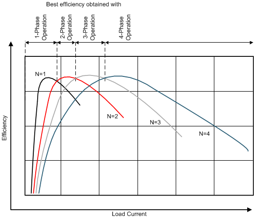
LP8758-B0 ai_eff4ph_SNVSA05.gifFigure 9. Multi-Phase Buck Converter Efficiency vs Number of Phases -
All Converters in PWM Mode (2)
Graph is not in scale and is for illustrative purposes only.