SNVSA50C August 2015 – May 2017 LP8861-Q1
PRODUCTION DATA.
- 1 Features
- 2 Applications
- 3 Description
- 4 Revision History
- 5 Device Comparison Table
- 6 Pin Configuration and Functions
-
7 Specifications
- 7.1 Absolute Maximum Ratings
- 7.2 ESD Ratings
- 7.3 Recommended Operating Conditions
- 7.4 Thermal Information
- 7.5 Electrical Characteristics
- 7.6 Internal LDO Electrical Characteristics
- 7.7 Protection Electrical Characteristics
- 7.8 Power Line FET Control Electrical Characteristics
- 7.9 Current Sinks Electrical Characteristics
- 7.10 PWM Brightness Control Electrical Characteristics
- 7.11 Boost/SEPIC Converter Characteristics
- 7.12 Logic Interface Characteristics
- 7.13 Typical Characteristics
-
8 Detailed Description
- 8.1 Overview
- 8.2 Functional Block Diagram
- 8.3 Feature Description
- 8.4 Device Functional Modes
-
9 Application and Implementation
- 9.1 Application Information
- 9.2 Typical Applications
- 10Power Supply Recommendations
- 11Layout
- 12Device and Documentation Support
- 13Mechanical, Packaging, and Orderable Information
Package Options
Mechanical Data (Package|Pins)
- PWP|20
Thermal pad, mechanical data (Package|Pins)
- PWP|20
Orderable Information
8 Detailed Description
8.1 Overview
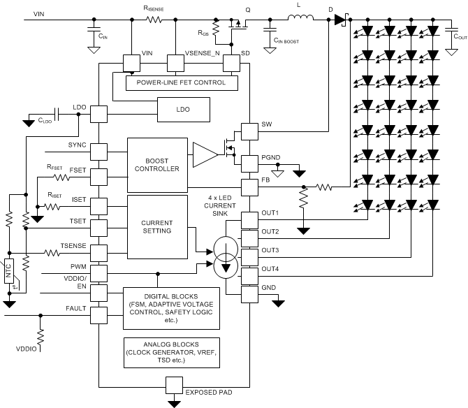
The LP8861-Q1 is a highly integrated LED driver for automotive infotainment, lighting systems, and medium-sized LCD backlight applications. It includes a boost/SEPIC converter with an integrated FET, an internal LDO, and four LED current sinks. A VDDIO/EN pin provides the supply voltage for digital IOs (PWM and SYNC inputs) and at the same time enables the device.
The switching frequency on the boost/SEPIC regulator is set by a resistor connected to the FSET pin. The maximum voltage is set by a resistive divider connected to the FB pin. For the best efficiency the voltage is adapted automatically to the minimum necessary level needed to drive the LED strings. This is done by monitoring LED output voltage in real time. For EMI reduction and control two optional features are available:
- Spread spectrum, which reduces EMI noise spikes at the switching frequency and its harmonic frequencies.
- Boost/SEPIC can be synchronized to an external clock frequency connected to the SYNC pin.
The four constant current sinks for driving the LEDs provide current up to 100 mA per sink and can be tied together to get a higher current. Value for the current value is set with a resistor connected to the ISET pin. Current sinks that are not used must be connected to the ground. Grounded current sinks are disabled and excluded from the adaptive voltage and open/short LED fault detection loop.
Brightness is controlled with the PWM input. Frequency range for the input PWM is from 100 Hz to 20 kHz. LED output PWM follows the input PWM so the output frequency is equal to the input frequency.
The LP8861-Q1 has extensive fault detection features:
- Open-string and shorted LED detections
- LED fault detection prevents system overheating in case of open or short in some of the LED strings
- VIN input-overvoltage protection
- Threshold sensing from VIN pin
- VIN input undervoltage protection
- Threshold sensing from VIN pin
- VIN input overcurrent protection
- Threshold sensing across RISENSE resistor
- Thermal shutdown in case of die overtemperature
- LED thermal protection with a external NTC (optional feature)
Fault condition is indicated with the FAULT output pin. Additionally, the LP8861-Q1 supports control for an optional power-line FET allowing further protection in boost/SEPIC overcurrent state by disconnecting the device from power-line in fault condition. With the power-line FET control it is possible to protect device, boost components, and LEDs in case of shorted VBOOST and too-high VIN voltage. Power-line FET control also features soft-start which reduces the peak current from the power line during start-up.
8.2 Functional Block Diagram
8.3 Feature Description
8.3.1 Integrated Boost/SEPIC Converter
The LP8861-Q1 boost/SEPIC DC-DC converter generates supply voltage for the LEDs. The maximum output voltage VMAX BOOST is defined by an external resistive divider (R1, R2).
Maximum voltage must be chosen based on the maximum voltage required for LED strings. Recommended VMAX BOOST is about 30% higher than maximum LED string voltage. DC-DC output voltage is adjusted automatically based on LED current sink headroom voltage. Maximum, minimum, and initial boost voltages can be calculated with Equation 1:

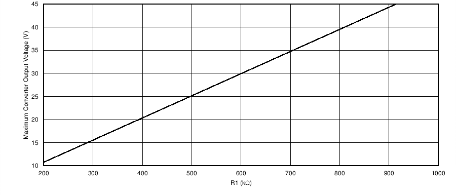 Figure 9. Maximum Converter Output Voltage vs R1 Resistance
Alternatively, a T-divider can be used if resistance less than 100 kΩ is required for the external resistive divider. Refer to LP8861-Q1EVM Evaluation Module for details.
The converter is a current mode DC-DC converter, where the inductor current is measured and controlled with the feedback. Switching frequency is adjustable between 300 kHz and 2.2 MHz with RFSET resistor as shown in Equation 2:
where
- ƒSW is switching frequency, kHz
- RFSET is frequency setting resistor, kΩ
In most cases lower frequency has higher system efficiency. Boost parameters are chosen automatically during start-up according to the selected switching frequency (see Table 2). In boost mode a 15-pF capacitor CFB must be placed across resistor R1 when operating in 300 kHz ... 500 kHz range (see Figure 24). When operating in the 1.8-MHz...2.2-MHz range, CFB = 4.7 pF (see Figure 29).
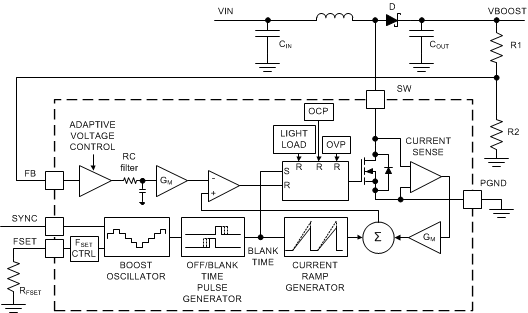 Figure 10. Boost Block Diagram
Boost clock can be driven by an external SYNC signal between 300 kHz…2.2 MHz. If the external synchronization input disappears, boost continues operation at the frequency defined by RFSET resistor. When external frequency disappears and SYNC pin level is low, boost continues operation without spread spectrum immediately. If SYNC remains high, boost continues switching with spread spectrum enabled after 256 µs.
External SYNC frequency must be 1.2…1.5 times higher than the frequency defined by the RFSET resistor. Minimum frequency setting with RFSET is 250 kHz to support minimum switching frequency with external clock frequency 300 kHz.
The optional spread-spectrum feature (±3% from central frequency, 1-kHz modulation frequency) reduces EMI noise spikes at the switching frequency and its harmonic frequencies. When external synchronization is used, spread spectrum is not available.
Table 1. Boost Synchronization Mode
| SYNC PIN STATUS | MODE |
|---|---|
| Low | Spread spectrum disabled |
| High | Spread spectrum enabled |
| 300...2200 kHz frequency | Spread spectrum disabled, external synchronization mode |
Table 2. Boost Parameters(1)
| RANGE | FREQUENCY (kHz) | TYPICAL INDUCTANCE (µH) |
TYPICAL BOOST INPUT AND OUTPUT CAPACITORS (µF) |
MIN SWITCH OFF TIME (ns)(2) |
BLANK TIME (ns) |
CURRENT RAMP (A/s) |
CURRENT RAMP DELAY (ns) |
|---|---|---|---|---|---|---|---|
| 1 | 300...480 | 33 | 2 × 10 (cer.) + 33 (electr.) | 150 | 95 | 24 | 550 |
| 2 | 480...1150 | 15 | 10 (cer.) +33 (electr.) | 60 | 95 | 43 | 300 |
| 3 | 1150...1650 | 10 | 3 × 10 (cer.) | 40 | 95 | 79 | 0 |
| 4 | 1650...2200 | 4.7 | 3 × 10 (cer.) | 40 | 70 | 145 | 0 |
Boost SW pin DC current is limited to 2 A (typical). To support warm start transient condition the current limit is automatically increased to 2.5 A for a short period of 1.5 seconds when a 2-A limit is reached.
NOTE
Application condition where the 2-A limit is exceeded continuously is not allowed. In this case the current limit would be 2 A for 1.5 seconds followed by 2.5-A limit for 1.5 seconds, and this 3-second period repeats.
To keep switching voltage within safe levels there is a 48-V limit comparator in the event that FB loop is broken.
8.3.2 Internal LDO
The internal LDO regulator converts the input voltage at VIN to a 4.3-V output voltage. The LDO regulator supplies internal and external circuitry. The maximum external load is 5 mA. Connect LDO output with a minimum of 1-µF ceramic capacitor to ground as close to the LDO pin as possible. If an external voltage higher than 4.5 V is connected to LDO pin, the internal LDO is disabled, and the internal circuitry is powered from the external power supply. VIN and VSENSE_N pins must be connected to the same external voltage as LDO pin. See Figure 29 for application schematic example.
8.3.3 LED Current Sinks
8.3.3.1 Current Sink Configuration
The LP8861-Q1 detects LED current sinks configuration during start-up. Any sink connected to the ground is disabled and excluded from the adaptive boost control and fault detection.
8.3.3.2 Current Setting
Maximum current for the LED current sinks is controlled with external RISET resistor. RISET value for target maximum current can be calculated using Equation 3:
8.3.4 Power-Line FET Control
The LP8861-Q1 has a control pin (SD) for driving the gate of an external power-line FET. Power-line FET is an optional feature; an example schematic is shown in Figure 24. Power-line FET limits inrush current by turning on gradually when the device is enabled (VDDIO/EN = high, VIN > VGS). Inrush current is controlled by increasing sink current for the FET gradually to 230 μA.
In shutdown the LP8861-Q1 turns off the power-line FET and prevents the possible boost and LEDs leakage. The power switch also turns off in case of any fault which causes the device to enter FAULT RECOVERY state.
8.3.5 LED Current Dimming With External Temperature Sensor
The LP8861-Q1 has an optional feature to decrease automatically LED current when LED overheating is detected with an external NTC sensor. An example of the behavior is shown in Figure 11. When the NTC temperature reaches T1, the LP8861-Q1 starts to decrease the LED current. When the LED current has reduced to 17.5% of the nominal value, current turns off until temperature returns to the operation range. When TSET pin is grounded this feature is disabled. Temperature T1 and de-rate slope are defined by external resistors as explained below.
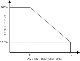 Figure 11. Temperature-Based LED Current Dimming Functionality
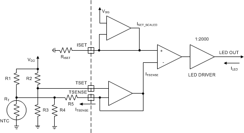 Figure 12. Temperature-Based LED Current Dimming Implementation
When the TSET pin is grounded LED current is set by RISET resistor:

When external NTC is connected, the TSENSE pin current decreases LED output current. The following steps describe how to calculate LED output current.
Parallel resistance of the NTC sensor RT and resistor R4 is calculated by formula:

TSET voltage can be calculated with Equation 6:

TSENSE pin current is calculated by Equation 7:

ISET pin current defined by RISET is:

For Equation 9, ITSENSE current must be limited between 0 and ISET_SCALED. If ITSENSE > ISET_SCALED then set ITSENSE = ISET_SCALED. If ITSENSE < 0 then set ITSENSE = 0.
LED driver output current is:
When current is lower than 17.5% of the nominal value, the current is set to 0 (so called cut-off point).
An Excel® calculator is available for calculating the component values for a specific NTC and target thermal profile (contact your local TI representative). Figure 13 shows an example thermal profile implementation.
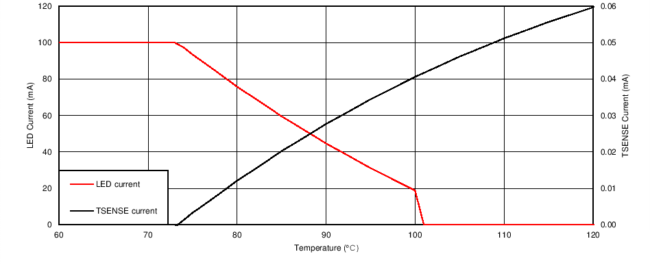
| NTC – 10 kΩ at 25ºC | RISET = 24 kΩ | R2 = 10 kΩ | R4 = 100 kΩ |
| VDD = 4.3 V | R1 = 10 kΩ | R3 = 2 kΩ | R5 = 7.5 kΩ |
8.3.6 Protection and Fault Detection
The LP8861-Q1 has fault detection for LED open and short, VIN input overvoltage (VIN_OVP), VIN undervoltage lockout (VIN_UVLO), power line overcurrent (VIN_OCP), and thermal shutdown (TSD).
8.3.6.1 Adaptive Boost Control and Functionality of LED Fault Comparators
Adaptive boost control function adjusts the boost output voltage to the minimum sufficient voltage for proper LED current sink operation. The output with highest VF LED string is detected and boost output voltage adjusted accordingly. Boost adaptive control voltage step size is defined by maximum boost voltage settings, VSTEP = (VMAX BOOST - VMIN BOOST) / 256. Periodic down pressure is applied to the target boost voltage to achieve better system efficiency.
Every LED current sink has 3 comparators for an adaptive boost control and fault detection. Comparator outputs are filtered, filtering time is 1 µs.
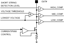 Figure 14. Comparators for Adaptive Voltage Control and LED Fault Detection
Figure 15 illustrates different cases which cause boost voltage increase, decrease, or generate faults. In normal operation, voltage at all the OUT# pins is between LOW_COMP and MID_COMP levels and boost voltage stays constant. LOW_COMP level is the minimum for proper LED current sink operation, 1.1 × VSAT + 0.2 V (typical). MID_COMP level is 1.1 × VSAT + 1.2 V (typical) — that is, typical headroom window is 1 V.
When voltage at all the OUT# pins increases above MID_COMP level, boost voltage adapts downwards.
When voltage at any of the OUT# pins falls below LOW_COMP threshold, boost voltage adapts upwards. In the condition where boost voltage reaches the maximum and there are one or more outputs still below LOW_COMP level, an open LED fault is detected.
HIGH_COMP level, 6 V typical, is the threshold for shorted LED detection. When the voltage of one or more of the OUT# pins increases above HIGH_COMP level and at least one of the other outputs is within the normal headroom window, shorted LED fault is detected.
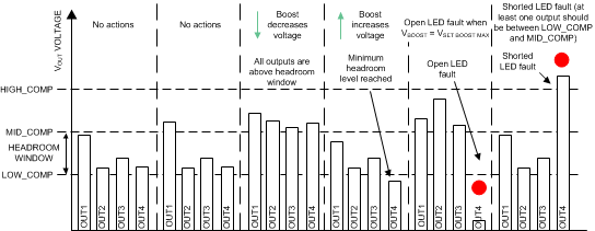 Figure 15. Boost Adaptation and LED Protection Algorithms
8.3.6.2 Overview of the Fault/Protection Schemes
The LP8861-Q1 fault detection behavior is described in Table 3. Detected faults (excluding LED faults) cause the device to enter FAULT_RECOVERY state. In FAULT_RECOVERY the boost and LED outputs of LP8861-Q1 are disabled, power-line FET is turned off, and the FAULT pin is pulled low. Device recovers automatically and enters normal operating mode (ACTIVE) after a recovery time of 100 ms if the fault condition has disappeared. When recovery is successful, the FAULT pin is released.
In case a LED fault is detected, device continues normal operation and only the faulty string is disabled. Fault is indicated via FAULT pin which can be released by toggling VDDIO/EN pin low for a short period of 2…20 µs. LEDs are turned off for this period but device stays in ACTIVE mode. If VDDIO/EN is low longer, device goes to STANDBY and restarts when EN goes high again.
Table 3. Fault/Protection Schemes
| FAULT/ PROTECTION |
FAULT NAME | THRESHOLD | CONNECTED TO FAULT PIN |
FAULT_ RECOVERY STATE |
ACTION |
|---|---|---|---|---|---|
| VIN overvoltage protection | VIN_OVP | 1. VIN > 42 V
2. VBOOST > VSET_BOOST + (6...10) V VSET_BOOST is voltage value defined by logic during adaptation |
Yes | Yes | 1. Overvoltage is monitored from the beginning of soft start. Fault is detected if the duration of overvoltage condition is 100 µs minimum. 2. Overvoltage is monitored from the beginning of normal operation (ACTIVE mode). Fault is detected if overvoltage condition duration is 560 ms minimum (tfilter). After the first fault detection filter time is reduced to 50 ms for following recovery cycles. When device recovers and has been in ACTIVE mode for 160 ms, filter is increased back to 560 ms. |
| VIN undervoltage lockout | VIN_UVLO | Falling 3.9 V Rising 4 V |
Yes | Yes | Detects undervoltage condition at VIN pin. Sensed from the beginning of soft start. Fault is detected if undervoltage condition duration is 100 µs minimum. |
| VIN overcurrent protection | VIN_OCP | 3 A (50-mΩ current sensor resistor) | Yes | Yes | Detects overcurrent by measuring voltage of the SENSE resistor connected between VIN and VSENSE_N pins. Sensed from the beginning of soft start. Fault is detected if undervoltage condition duration is 10 µs minimum. |
| Open LED fault | OPEN_LED | LOW_COMP threshold | Yes | No | Detected if one or more outputs are below threshold level, and boost adaptive control has reached maximum voltage. Open string(s) is removed from voltage control loop and PWM is disabled. Fault pin is cleaned by toggling VDDIO/EN pin. If VDDIO/EN is low for a short period of 2…20 µs, LEDs are turned off for this period but device stays ACTIVE. If VDDIO/EN is low longer, device goes to STANDBY and restarts when EN goes high again. |
| Shorted LED fault | SHORT_LED | Shorted string detection level 6 V | Yes | No | Detected if one or more outputs voltages are above shorted string detection level and at least one LED output voltage is within headroom window. Shorted string(s) are removed from the boost voltage control loop and outputs PWM(s) are disabled. Fault pin is cleaned by toggling VDDIO/EN pin. If VDDIO/EN is low for a short period of 2…20 µs, LEDs are turned off for this period but device stays ACTIVE. If VDDIO/EN is low longer, device goes to STANDBY and restarts when EN goes high again. |
| Thermal protection | TSD | 165ºC Thermal Shutdown Hysteresis 20ºC |
Yes | Yes | Thermal shutdown is monitored from the beginning of soft start. Die temperature must decrease by 20ºC for device to recover. |
 Figure 16. VIN Overvoltage Protection (Boost OVP)
 Figure 17. VIN Overvoltage Protection (VIN OVP)
 Figure 18. VIN Undervoltage Lockout
 Figure 19. Input Voltage Overcurrent Protection
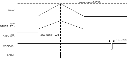 Figure 20. LED Open Fault
 Figure 21. LED Short Fault
8.4 Device Functional Modes
8.4.1 Device States
The LP8861-Q1 enters STANDBY mode when the internal LDO output rises above the power-on reset level, VLDO > VPOR_R. In STANDBY mode device is able to detect the VDDIO/EN signal. When VDDIO/EN is pulled high, device powers up. During soft start the external power line FET is opened gradually to limit inrush current. Soft start is followed by boost start, during which time boost voltage is ramped to the initial value. After boost start LED outputs are sensed to detect grounded current sinks. Grounded current sinks are disabled and excluded from the boost voltage control loop.
If a fault condition is detected, the LP8861-Q1 enters FAULT_RECOVERY state. In this state power line FET is switched off and both the boost and LED current sinks are disabled. Fault that cause the device to enter FAULT_RECOVERY are listed in Figure 22. When LED open or short is detected, faulty string is disabled but LP8861-Q1 stays in ACTIVE mode.
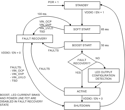 Figure 22. State Diagram
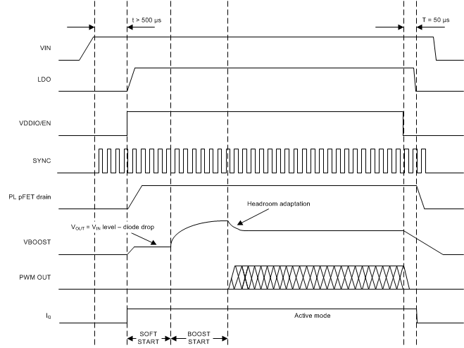 Figure 23. Timing Diagram for the Typical Start-Up and Shutdown