SNVSB83B June 2019 – January 2020 LP8867-Q1 , LP8869-Q1
PRODUCTION DATA.
- 1 Features
- 2 Applications
- 3 Description
- 4 Revision History
- 5 Device Comparison Table
- 6 Pin Configuration and Functions
-
7 Specifications
- 7.1 Absolute Maximum Ratings
- 7.2 ESD Ratings
- 7.3 Recommended Operating Conditions
- 7.4 Thermal Information
- 7.5 Electrical Characteristics
- 7.6 Internal LDO Electrical Characteristics
- 7.7 Protection Electrical Characteristics
- 7.8 Current Sinks Electrical Characteristics
- 7.9 PWM Brightness Control Electrical Characteristics
- 7.10 Boost and SEPIC Converter Characteristics
- 7.11 Logic Interface Characteristics
- 7.12 Typical Characteristics
-
8 Detailed Description
- 8.1 Overview
- 8.2 Functional Block Diagram
- 8.3
Feature Description
- 8.3.1 Integrated DC-DC Converter
- 8.3.2 Internal LDO
- 8.3.3 LED Current Sinks
- 8.3.4 Power-Line FET Control
- 8.3.5 LED Current Dimming With External Temperature Sensor
- 8.3.6 Fault Detections and Protection
- 8.4 Device Functional Modes
- 9 Application and Implementation
- 10Power Supply Recommendations
- 11Layout
- 12Device and Documentation Support
- 13Mechanical, Packaging, and Orderable Information
Package Options
Mechanical Data (Package|Pins)
- PWP|20
Thermal pad, mechanical data (Package|Pins)
- PWP|20
Orderable Information
8.3.5 LED Current Dimming With External Temperature Sensor
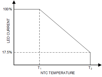
The LP886x-Q1 has an optional feature to decrease automatically LED current when LED overheating is detected with an external NTC sensor. An example of the behavior is shown in Figure 15. When the NTC temperature reaches T1, the LP886x-Q1 starts to decrease the LED current. When the LED current has reduced to 17.5% of the nominal value, current turns off until temperature returns to the operation range.
 Figure 15. Temperature-Based LED Current Dimming Functionality
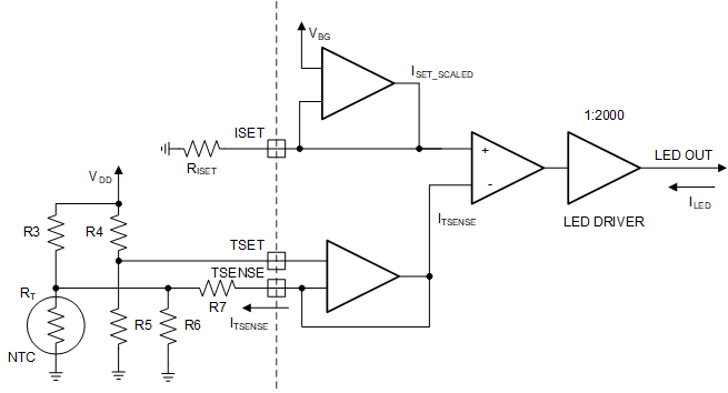
  Figure 16. Temperature-Based LED Current Dimming Implementation
 When TSET pin is grounded and TSENSE is floated, this feature is disabled. LED current is set by RISET resistor:

where
- VBG = 1.2 V
- RISET is current setting resistor, kΩ
- ILED is output current per OUTx pin, mA
When external NTC is connected, the TSENSE pin current decreases LED output current. Temperature T1 and de-rate slope are defined by external resistors as explained below.
Parallel resistance of the NTC sensor RT and resistor R4 is calculated by formula:

TSET voltage can be calculated with Equation 8:

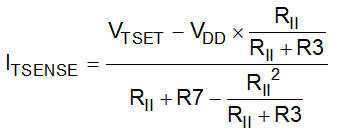
TSENSE pin current is calculated by Equation 9:

where
- VDD is the bias voltage of the resistor group. It's recommended to connect with chip's internal LDO output (pin 2)
ISET pin current defined by RISET is:

For Equation 11, ITSENSE current must be limited between 0 and ISET_SCALED. If ITSENSE > ISET_SCALED then set ITSENSE = ISET_SCALED. If ITSENSE < 0 then set ITSENSE = 0.
LED driver output current is:
When current is lower than 17.5% of the nominal value, the current is set to 0 (the cut-off point).
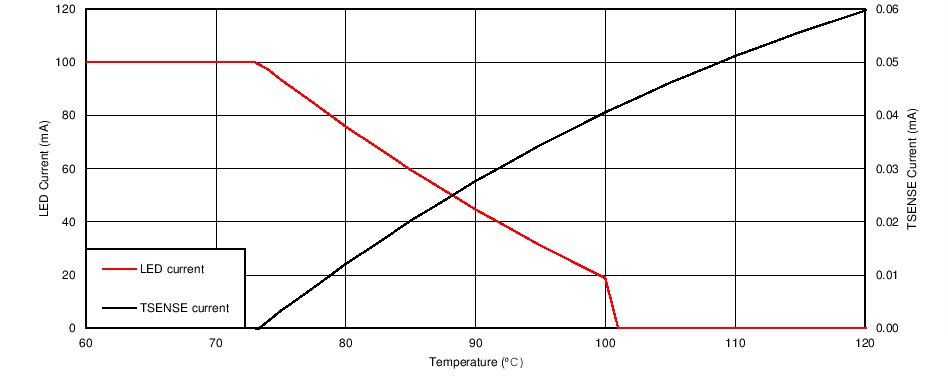
An Excel® calculator is available for calculating the component values for a specific NTC and target thermal profile (contact TI E2E™ support forums ). Figure 17 shows an example thermal profile implementation.

| NTC – 10 kΩ at 25ºC | RISET = 24 kΩ | R2 = 10 kΩ | R4 = 100 kΩ |
| VDD = 4.3 V | R1 = 10 kΩ | R3 = 2 kΩ | R5 = 7.5 kΩ |