SDLS969B may 2018 – may 2023 LSF0102-Q1
PRODUCTION DATA
- 1
- 1 Features
- 2 Applications
- 3 Description
- 4 Revision History
- 5 Pin Configuration and Functions
-
6 Specifications
- 6.1 Absolute Maximum Ratings
- 6.2 ESD Ratings
- 6.3 Recommended Operating Conditions
- 6.4 Thermal Information
- 6.5 Electrical Characteristics
- 6.6 Switching Characteristics (Translating Down): VCCB = 3.3 V
- 6.7 Switching Characteristics (Translating Down): VCCB = 2.5 V
- 6.8 Switching Characteristics Translating Up): VCCB = 3.3 V
- 6.9 Switching Characteristics (Translating Up): VCCB = 2.5 V
- 6.10 Typical Characteristics
- 7 Parameter Measurement Information
- 8 Detailed Description
- 9 Application and Implementation
- 10Device and Documentation Support
- 11Mechanical, Packaging, and Orderable Information
Package Options
Mechanical Data (Package|Pins)
- DCU|8
Thermal pad, mechanical data (Package|Pins)
Orderable Information
3 Description
The LSF0102-Q1 device is an auto bidirectional voltage translator that translates among a wide range of supplies without the need for a directional pin. The LSF0102-Q1 supports up to 100 MHz up translation and greater than 100 MHz down translation with capacitive loads ≤ 30 pF. Additionally, the LSF0102-Q1 supports up to 40 MHz up and down translation at 50 pF capacitance load, which enables the LSF0102-Q1 device to support a wide variety of standard interfaces commonly found in automotive applications such as I2C, SPI, GPIO, SDIO, UART, and MDIO.
The LSF0102-Q1 device has 5-V tolerant data inputs. This makes the device compatible with TTL voltage levels. Furthermore, the LSF0102-Q1 supports mixed-mode voltage translation, allowing the device to up translate and down translate to different supply levels on each channel.
| PART NUMBER | PACKAGE | BODY SIZE (NOM) |
|---|---|---|
| LSF0102-Q1 | DCU (VSSOP, 8) | 2.30 mm × 2.00 mm |
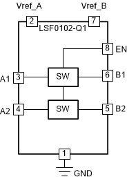
 Functional
Block Diagram