SLLS410O January 2000 – June 2021 MAX3232
PRODUCTION DATA
- 1 Features
- 2 Applications
- 3 Description
- 4 Revision History
- 5 Pin Configuration and Functions
- 6 Specifications
- 7 Parameter Measurement Information
- 8 Detailed Description
- 9 Application and Implementation
- 10Power Supply Recommendations
- 11Layout
- 12Device and Documentation Support
- 13Mechanical, Packaging, and Orderable Information
Package Options
Refer to the PDF data sheet for device specific package drawings
Mechanical Data (Package|Pins)
- DB|16
- PW|16
- DW|16
- D|16
Thermal pad, mechanical data (Package|Pins)
- DW|16
Orderable Information
3 Description
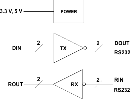
The MAX3232 device consists of two line drivers, two line receivers, and a dual charge-pump circuit with ±15-kV ESD protection terminal to terminal (serial-port connection terminals, including GND). The device meets the requirements of TIA/EIA-232-F and provides the electrical interface between an asynchronous communication controller and the serial-port connector. The charge pump and four small external capacitors allow operation from a single 3-V to 5.5-V supply. The devices operate at data signaling rates up to 250 kbit/s and a maximum of 30-V/μs driver output slew rate.
Device
Information
| PART NUMBER | PACKAGE(1) | BODY SIZE |
|---|---|---|
| MAX3232 | SOIC (D) (16) | 9.90 mm × 3.91 mm |
| SSOP (DB) (16) | 6.20 mm × 5.30 mm | |
| SOIC (DW) (16) | 10.30 mm × 7.50 mm | |
| TSSOP (PW) (16) | 5.00 mm × 4.40 mm |
(1) For all available packages, see the orderable addendum at the end of the data sheet.
 Simplified Schematic