SLAS639L July 2011 – December 2017 MSP430FR5730 , MSP430FR5731 , MSP430FR5732 , MSP430FR5733 , MSP430FR5734 , MSP430FR5735 , MSP430FR5736 , MSP430FR5737 , MSP430FR5738 , MSP430FR5739
PRODUCTION DATA.
- 1Device Overview
- 2Revision History
- 3Device Comparison
-
4Terminal Configuration and Functions
- 4.1 Pin Diagram - RHA Package - MSP430FR5731, MSP430FR5733, MSP430FR5735, MSP430FR5737, MSP430FR5739
- 4.2 Pin Diagram - DA Package - MSP430FR5731, MSP430FR5733, MSP430FR5735, MSP430FR5737, MSP430FR5739
- 4.3 Pin Diagram - RGE Package - MSP430FR5730, MSP430FR5732, MSP430FR5734, MSP430FR5736, MSP430FR5738
- 4.4 Pin Diagram - YQD Package - MSP430FR5738
- 4.5 Pin Diagram - PW Package - MSP430FR5730, MSP430FR5732, MSP430FR5734, MSP430FR5736, MSP430FR5738
- 4.6 Signal Descriptions
-
5Specifications
- 5.1 Absolute Maximum Ratings
- 5.2 ESD Ratings
- 5.3 Recommended Operating Conditions
- 5.4 Active Mode Supply Current Into VCC Excluding External Current
- 5.5 Low-Power Mode Supply Currents (Into VCC) Excluding External Current
- 5.6 Thermal Resistance Characteristics
- 5.7 Schmitt-Trigger Inputs - General-Purpose I/O (P1.0 to P1.7, P2.0 to P2.7, P3.0 to P3.7, P4.0 to P4.1, PJ.0 to PJ.5, RST/NMI)
- 5.8 Inputs - Ports P1 and P2 (P1.0 to P1.7, P2.0 to P2.7)
- 5.9 Leakage Current - General-Purpose I/O (P1.0 to P1.7, P2.0 to P2.7, P3.0 to P3.7, P4.0 to P4.1, PJ.0 to PJ.5, RST/NMI)
- 5.10 Outputs - General-Purpose I/O (P1.0 to P1.7, P2.0 to P2.7, P3.0 to P3.7, P4.0 to P4.1, PJ.0 to PJ.5)
- 5.11 Output Frequency - General-Purpose I/O (P1.0 to P1.7, P2.0 to P2.7, P3.0 to P3.7, P4.0 to P4.1, PJ.0 to PJ.5)
- 5.12 Typical Characteristics - Outputs
- 5.13 Crystal Oscillator, XT1, Low-Frequency (LF) Mode
- 5.14 Crystal Oscillator, XT1, High-Frequency (HF) Mode
- 5.15 Internal Very-Low-Power Low-Frequency Oscillator (VLO)
- 5.16 DCO Frequencies
- 5.17 MODOSC
- 5.18 PMM, Core Voltage
- 5.19 PMM, SVS, BOR
- 5.20 Wake-up Times From Low-Power Modes
- 5.21 Timer_A
- 5.22 Timer_B
- 5.23 eUSCI (UART Mode) Clock Frequency
- 5.24 eUSCI (UART Mode)
- 5.25 eUSCI (SPI Master Mode) Clock Frequency
- 5.26 eUSCI (SPI Master Mode)
- 5.27 eUSCI (SPI Slave Mode)
- 5.28 eUSCI (I2C Mode)
- 5.29 10-Bit ADC, Power Supply and Input Range Conditions
- 5.30 10-Bit ADC, Timing Parameters
- 5.31 10-Bit ADC, Linearity Parameters
- 5.32 REF, External Reference
- 5.33 REF, Built-In Reference
- 5.34 REF, Temperature Sensor and Built-In VMID
- 5.35 Comparator_D
- 5.36 FRAM
- 5.37 JTAG and Spy-Bi-Wire Interface
-
6Detailed Description
- 6.1 Functional Block Diagrams
- 6.2 CPU
- 6.3 Operating Modes
- 6.4 Interrupt Vector Addresses
- 6.5 Memory Organization
- 6.6 Bootloader (BSL)
- 6.7 JTAG Operation
- 6.8 FRAM
- 6.9 Memory Protection Unit (MPU)
- 6.10
Peripherals
- 6.10.1 Digital I/O
- 6.10.2 Oscillator and Clock System (CS)
- 6.10.3 Power-Management Module (PMM)
- 6.10.4 Hardware Multiplier (MPY)
- 6.10.5 Real-Time Clock (RTC_B)
- 6.10.6 Watchdog Timer (WDT_A)
- 6.10.7 System Module (SYS)
- 6.10.8 DMA Controller
- 6.10.9 Enhanced Universal Serial Communication Interface (eUSCI)
- 6.10.10 TA0, TA1
- 6.10.11 TB0, TB1, TB2
- 6.10.12 ADC10_B
- 6.10.13 Comparator_D
- 6.10.14 CRC16
- 6.10.15 Shared Reference (REF)
- 6.10.16 Embedded Emulation Module (EEM)
- 6.10.17 Peripheral File Map
- 6.11
Input/Output Diagrams
- 6.11.1 Port P1 (P1.0 to P1.2) Input/Output With Schmitt Trigger
- 6.11.2 Port P1 (P1.3 to P1.5) Input/Output With Schmitt Trigger
- 6.11.3 Port P1 (P1.6 and P1.7) Input/Output With Schmitt Trigger
- 6.11.4 Port P2 (P2.0 to P2.2) Input/Output With Schmitt Trigger
- 6.11.5 Port P2 (P2.3 and P2.4) Input/Output With Schmitt Trigger
- 6.11.6 Port P2 (P2.5 and P2.6) Input/Output With Schmitt Trigger
- 6.11.7 Port P2 (P2.7) Input/Output With Schmitt Trigger
- 6.11.8 Port P3 (P3.0 to P3.3) Input/Output With Schmitt Trigger
- 6.11.9 Port P3 (P3.4 to P3.6) Input/Output With Schmitt Trigger
- 6.11.10 Port Port P3 (P3.7) Input/Output With Schmitt Trigger
- 6.11.11 Port Port P4 (P4.0) Input/Output With Schmitt Trigger
- 6.11.12 Port Port P4 (P4.1) Input/Output With Schmitt Trigger
- 6.11.13 Port Port PJ (PJ.0 to PJ.3) JTAG Pins TDO, TMS, TCK, TDI/TCLK, Input/Output With Schmitt Trigger or Output
- 6.11.14 Port Port PJ (PJ.4 and PJ.5) Input/Output With Schmitt Trigger
- 6.12 Device Descriptors (TLV)
- 7Device and Documentation Support
- 8Mechanical, Packaging, and Orderable Information
Package Options
Mechanical Data (Package|Pins)
Thermal pad, mechanical data (Package|Pins)
- RGE|24
Orderable Information
6 Detailed Description
6.1 Functional Block Diagrams
Figure 6-1 shows the functional block diagram for the MSP430FR5731, MSP430FR5735, and MSP430FR5739 in the RHA package.
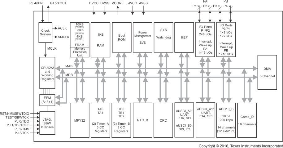 Figure 6-1 Functional Block Diagram – RHA Package – MSP430FR5731, MSP430FR5735, MSP430FR5739
Figure 6-2 shows the functional block diagram for the MSP430FR5733 and MSP430FR5737 devices in the RHA package.
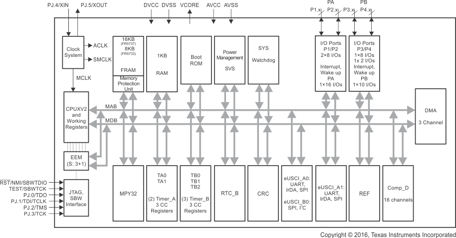 Figure 6-2 Functional Block Diagram – RHA Package – MSP430FR5733, MSP430FR5737
Figure 6-3 shows the functional block diagram for the MSP430FR5731, MSP430FR5735, and MSP430FR5739 devices in the DA package.
 Figure 6-3 Functional Block Diagram – DA Package – MSP430FR5731, MSP430FR5735, MSP430FR5739
Figure 6-4 shows the functional block diagram for the MSP430FR5733 and MSP430FR5737 devices in the DA package.
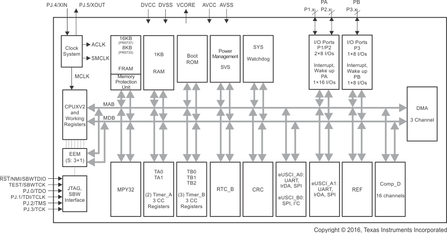 Figure 6-4 Functional Block Diagram – DA Package – MSP430FR5733, MSP430FR5737
Figure 6-5 shows the functional block diagram for the MSP430FR5730, MSP430FR5734, and MSP430FR5738 devices in the RGE and YQD packages.
 Figure 6-5 Functional Block Diagram – RGE or YQD (FR5738 Only) Package – MSP430FR5730, MSP430FR5734, MSP430FR5738
Figure 6-6 shows the functional block diagram for the MSP430FR5732 and MSP430FR5736 devices in the RGE package.
 Figure 6-6 Functional Block Diagram – RGE Package – MSP430FR5732, MSP430FR5736
Figure 6-7 shows the functional block diagram for the MSP430FR5730, MSP430FR5734, and MSP430FR5738 devices in the PW package.
 Figure 6-7 Functional Block Diagram – PW Package – MSP430FR5730, MSP430FR5734, MSP430FR5738
Figure 6-8 shows the functional block diagram for the MSP430FR5732 and MSP430FR5736 devices in the PW package.
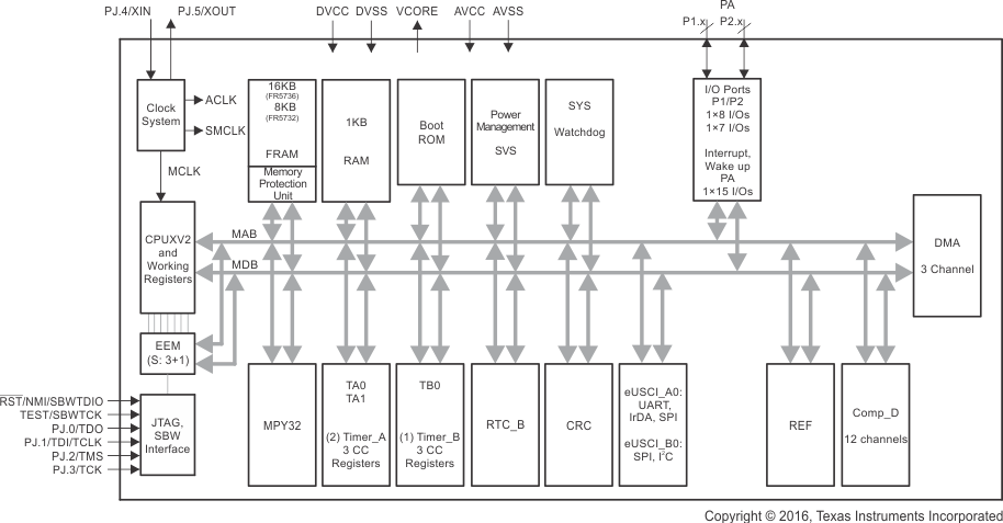 Figure 6-8 Functional Block Diagram – PW Package – MSP430FR5732, MSP430FR5736
6.2 CPU
The MSP430 CPU has a 16-bit RISC architecture that is highly transparent to the application. All operations, other than program-flow instructions, are performed as register operations in conjunction with seven addressing modes for source operand and four addressing modes for destination operand.
The CPU is integrated with 16 registers that provide reduced instruction execution time. The register-to-register operation execution time is one cycle of the CPU clock.
Four of the registers, R0 to R3, are dedicated as program counter, stack pointer, status register, and constant generator, respectively. The remaining registers are general-purpose registers.
Peripherals are connected to the CPU using data, address, and control buses, and can be handled with all instructions.
The instruction set consists of the original 51 instructions with three formats and seven address modes and additional instructions for the expanded address range. Each instruction can operate on word and byte data.
6.3 Operating Modes
The MSP430 has one active mode and seven software-selectable low-power modes of operation. An interrupt event can wake up the device from low-power modes LPM0 through LPM4, service the request, and restore back to the low-power mode on return from the interrupt program. Low-power modes LPM3.5 and LPM4.5 disable the core supply to minimize power consumption.
The following eight operating modes can be configured by software:
- Active mode (AM)
- All clocks are active
- Low-power mode 0 (LPM0)
- CPU is disabled
- ACLK active
- MCLK disabled
- SMCLK optionally active
- Complete data retention
- Low-power mode 1 (LPM1)
- CPU is disabled
- ACLK active
- MCLK disabled
- SMCLK optionally active
- DCO disabled
- Complete data retention
- Low-power mode 2 (LPM2)
- CPU is disabled
- ACLK active
- MCLK disabled
- SMCLK optionally active
- DCO disabled
- Complete data retention
- Low-power mode 3 (LPM3)
- CPU is disabled
- ACLK active
- MCLK and SMCLK disabled
- DCO disabled
- Complete data retention
- Low-power mode 4 (LPM4)
- CPU is disabled
- ACLK, MCLK, SMCLK disabled
- Complete data retention
- Low-power mode 3.5 (LPM3.5)
- RTC operation
- Internal regulator disabled
- No data retention
- I/O pad state retention
- Wake-up input from RST, general-purpose I/O, RTC events
- Low-power mode 4.5 (LPM4.5)
- Internal regulator disabled
- No data retention
- I/O pad state retention
- Wake-up input from RST and general-purpose I/O
6.4 Interrupt Vector Addresses
The interrupt vectors and the power-up start address are in the address range 0FFFFh to 0FF80h (see Table 6-1). The vector contains the 16-bit address of the appropriate interrupt-handler instruction sequence.
Table 6-1 Interrupt Sources, Flags, and Vectors
| INTERRUPT SOURCE | INTERRUPT FLAG | SYSTEM INTERRUPT | WORD ADDRESS | PRIORITY |
|---|---|---|---|---|
| System Reset
Power-Up, Brownout, Supply Supervisors External Reset RST Watchdog Time-out (Watchdog mode) WDT, FRCTL MPU, CS, PMM Password Violation FRAM double bit error detection MPU segment violation Software POR, BOR |
SVSLIFG, SVSHIFG PMMRSTIFG WDTIFG WDTPW, FRCTLPW, MPUPW, CSPW, PMMPW DBDIFG MPUSEGIIFG, MPUSEG1IFG, MPUSEG2IFG, MPUSEG3IFG PMMPORIFG, PMMBORIFG (SYSRSTIV) (1) (3) |
Reset | 0FFFEh | 63, highest |
| System NMI
Vacant Memory Access JTAG Mailbox FRAM access time error FRAM single, double bit error detection |
VMAIFG JMBNIFG, JMBOUTIFG ACCTIMIFG SBDIFG, DBDIFG (SYSSNIV) (1) |
(Non)maskable | 0FFFCh | 62 |
| User NMI
External NMI Oscillator Fault |
NMIIFG, OFIFG (SYSUNIV) (1) (3) |
(Non)maskable | 0FFFAh | 61 |
| Comparator_D | Comparator_D interrupt flags (CBIV) (1) (2) |
Maskable | 0FFF8h | 60 |
| TB0 | TB0CCR0 CCIFG0 (2) | Maskable | 0FFF6h | 59 |
| TB0 | TB0CCR1 CCIFG1 to TB0CCR2 CCIFG2, TB0IFG (TB0IV) (1) (2) |
Maskable | 0FFF4h | 58 |
| Watchdog Timer (Interval Timer Mode) |
WDTIFG | Maskable | 0FFF2h | 57 |
| eUSCI_A0 Receive and Transmit | UCA0RXIFG, UCA0TXIFG (SPI mode) UCA0STTIFG, UCA0TXCPTIFG, UCA0RXIFG, UXA0TXIFG (UART mode) (UCA0IV) (1) (2) |
Maskable | 0FFF0h | 56 |
| eUSCI_B0 Receive and Transmit | UCB0STTIFG, UCB0TXCPTIFG, UCB0RXIFG, UCB0TXIFG (SPI mode) UCB0ALIFG, UCB0NACKIFG, UCB0STTIFG, UCB0STPIFG, UCB0RXIFG0, UCB0TXIFG0, UCB0RXIFG1, UCB0TXIFG1, UCB0RXIFG2, UCB0TXIFG2, UCB0RXIFG3, UCB0TXIFG3, UCB0CNTIFG, UCB0BIT9IFG (I2C mode) (UCB0IV) (1) (2) |
Maskable | 0FFEEh | 55 |
| ADC10_B | ADC10OVIFG, ADC10TOVIFG, ADC10HIIFG, ADC10LOIFG ADC10INIFG, ADC10IFG0 (ADC10IV) (1) (2) (5) |
Maskable | 0FFECh | 54 |
| TA0 | TA0CCR0 CCIFG0 (2) | Maskable | 0FFEAh | 53 |
| TA0 | TA0CCR1 CCIFG1 to TA0CCR2 CCIFG2, TA0IFG (TA0IV) (1) (2) |
Maskable | 0FFE8h | 52 |
| eUSCI_A1 Receive and Transmit | UCA1RXIFG, UCA1TXIFG (SPI mode) UCA1STTIFG, UCA1TXCPTIFG, UCA1RXIFG, UXA1TXIFG (UART mode) (UCA1IV) (1) (2) |
Maskable | 0FFE6h | 51 |
| DMA | DMA0IFG, DMA1IFG, DMA2IFG (DMAIV) (1) (2) |
Maskable | 0FFE4h | 50 |
| TA1 | TA1CCR0 CCIFG0 (2) | Maskable | 0FFE2h | 49 |
| TA1 | TA1CCR1 CCIFG1 to TA1CCR2 CCIFG2, TA1IFG (TA1IV) (1) (2) |
Maskable | 0FFE0h | 48 |
| I/O Port P1 | P1IFG.0 to P1IFG.7 (P1IV) (1) (2) |
Maskable | 0FFDEh | 47 |
| TB1 | TB1CCR0 CCIFG0 (2) | Maskable | 0FFDCh | 46 |
| TB1 | TB1CCR1 CCIFG1 to TB1CCR2 CCIFG2, TB1IFG (TB1IV) (1) (2) |
Maskable | 0FFDAh | 45 |
| I/O Port P2 | P2IFG.0 to P2IFG.7 (P2IV) (1) (2) |
Maskable | 0FFD8h | 44 |
| TB2 | TB2CCR0 CCIFG0 (2) | Maskable | 0FFD6h | 43 |
| TB2 | TB2CCR1 CCIFG1 to TB2CCR2 CCIFG2, TB2IFG (TB2IV) (1) (2) |
Maskable | 0FFD4h | 42 |
| I/O Port P3 | P3IFG.0 to P3IFG.7 (P3IV) (1) (2) |
Maskable | 0FFD2h | 41 |
| I/O Port P4 | P4IFG.0 to P4IFG.2 (P4IV) (1) (2) |
Maskable | 0FFD0h | 40 |
| RTC_B | RTCRDYIFG, RTCTEVIFG, RTCAIFG, RT0PSIFG, RT1PSIFG, RTCOFIFG (RTCIV) (1) (2) |
Maskable | 0FFCEh | 39 |
| Reserved | Reserved (4) | 0FFCCh | 38 | |
| ⋮ | ⋮ | |||
| 0FF80h | 0, lowest |
(Non)maskable: the individual interrupt-enable bit can disable an interrupt event, but the general-interrupt enable cannot disable it.
6.5 Memory Organization
Table 6-2 describes the memory organization for all device variants.
Table 6-2 Memory Organization(1)(2)
| MSP430FR5736 MSP430FR5737 MSP430FR5738 MSP430FR5739 |
MSP430FR5732 MSP430FR5733 MSP430FR5734 MSP430FR5735 |
MSP430FR5730 MSP430FR5731 |
||
|---|---|---|---|---|
| Memory (FRAM) Main: interrupt vectors Main: code memory |
Total Size | 15.5KB 00FFFFh–00FF80h 00FF7Fh–00C200h |
8.0KB 00FFFFh–00FF80h 00FF7Fh–00E000h |
4KB 00FFFFh–00FF80h 00FF7Fh–00F000h |
| RAM | 1KB 001FFFh–001C00h |
1KB 001FFFh–001C00h |
1KB 001FFFh–001C00h |
|
| Device Descriptor Info (TLV) (FRAM) | 128 B 001A7Fh–001A00h |
128 B 001A7Fh–001A00h |
128 B 001A7Fh–001A00h |
|
| Information memory (FRAM) | N/A | 0019FFh–001980h Address space mirrored to Info A |
0019FFh–001980h Address space mirrored to Info A |
0019FFh–001980h Address space mirrored to Info A |
| N/A | 00197Fh–001900h Address space mirrored to Info B |
00197Fh–001900h Address space mirrored to Info B |
00197Fh–001900h Address space mirrored to Info B |
|
| Info A | 128 B 0018FFh–001880h |
128 B 0018FFh–001880h |
128 B 0018FFh–001880h |
|
| Info B | 128 B 00187Fh–001800h |
128 B 00187Fh–001800h |
128 B 00187Fh–001800h |
|
| Bootloader (BSL) memory (ROM) | BSL 3 | 512 B 0017FFh–001600h |
512 B 0017FFh–001600h |
512 B 0017FFh–001600h |
| BSL 2 | 512 B 0015FFh–001400h |
512 B 0015FFh–001400h |
512 B 0015FFh–001400h |
|
| BSL 1 | 512 B 0013FFh–001200h |
512 B 0013FFh–001200h |
512 B 0013FFh–001200h |
|
| BSL 0 | 512 B 0011FFh–001000h |
512 B 0011FFh–001000h |
512 B 0011FFh–001000h |
|
| Peripherals | Size | 4KB 000FFFh–0h |
4KB 000FFFh–0h |
4KB 000FFFh–0h |
6.6 Bootloader (BSL)
The BSL enables users to program the FRAM or RAM using a UART serial interface. Access to the device memory by the BSL is protected by an user-defined password. Use of the BSL requires four pins (see Table 6-3). BSL entry requires a specific entry sequence on the RST/NMI/SBWTDIO and TEST/SBWTCK pins. For complete description of the features of the BSL and its implementation, see the MSP430 Programming With the Bootloader User's Guide.
Table 6-3 BSL Pin Requirements and Functions
| DEVICE SIGNAL | BSL FUNCTION |
|---|---|
| RST/NMI/SBWTDIO | Entry sequence signal |
| TEST/SBWTCK | Entry sequence signal |
| P2.0 | Data transmit |
| P2.1 | Data receive |
| VCC | Power supply |
| VSS | Ground supply |
6.7 JTAG Operation
6.7.1 JTAG Standard Interface
The MSP430 family supports the standard JTAG interface, which requires four signals for sending and receiving data. The JTAG signals are shared with general-purpose I/O. The TEST/SBWTCK pin is used to enable the JTAG signals. In addition to these signals, the RST/NMI/SBWTDIO is required to interface with MSP430 development tools and device programmers. Table 6-4 lists the JTAG pin requirements. For further details on interfacing to development tools and device programmers, see the MSP430 Hardware Tools User's Guide. For a complete description of the features of the JTAG interface and its implementation, see MSP430 Programming Via the JTAG Interface.
Table 6-4 JTAG Pin Requirements and Functions
| DEVICE SIGNAL | DIRECTION | FUNCTION |
|---|---|---|
| PJ.3/TCK | IN | JTAG clock input |
| PJ.2/TMS | IN | JTAG state control |
| PJ.1/TDI/TCLK | IN | JTAG data input, TCLK input |
| PJ.0/TDO | OUT | JTAG data output |
| TEST/SBWTCK | IN | Enable JTAG pins |
| RST/NMI/SBWTDIO | IN | External reset |
| VCC | Power supply | |
| VSS | Ground supply |
6.7.2 Spy-Bi-Wire Interface
In addition to the standard JTAG interface, the MSP430 family supports the 2-wire Spy-Bi-Wire interface. Spy-Bi-Wire can be used to interface with MSP430 development tools and device programmers. Table 6-5 lists the Spy-Bi-Wire interface pin requirements. For further details on interfacing to development tools and device programmers, see the MSP430 Hardware Tools User's Guide. For a complete description of the features of the JTAG interface and its implementation, see MSP430 Programming Via the JTAG Interface.
Table 6-5 Spy-Bi-Wire Pin Requirements and Functions
| DEVICE SIGNAL | DIRECTION | FUNCTION |
|---|---|---|
| TEST/SBWTCK | IN | Spy-Bi-Wire clock input |
| RST/NMI/SBWTDIO | IN, OUT | Spy-Bi-Wire data input and output |
| VCC | Power supply | |
| VSS | Ground supply |
6.8 FRAM
The FRAM can be programmed through the JTAG port, Spy-Bi-Wire (SBW), the BSL, or in-system by the CPU. Features of the FRAM include:
- Low-power ultra-fast write nonvolatile memory
- Byte and word access capability
- Programmable and automated wait state generation
- Error correction coding (ECC) with single bit detection and correction, double bit detection
For important software design information regarding FRAM including but not limited to partitioning the memory layout according to application-specific code, constant, and data space requirements, the use of FRAM to optimize application energy consumption, and the use of the memory protection unit (MPU) to maximize application robustness by protecting the program code against unintended write accesses, see MSP430™ FRAM Technology – How To and Best Practices.
6.9 Memory Protection Unit (MPU)
The FRAM can be protected from inadvertent CPU execution or write access by the MPU. Features of the MPU include:
- Main memory partitioning programmable up to three segments
- Access rights for each segment (main and information memory) can be individually selected
- Access violation flags with interrupt capability for easy servicing of access violations
6.10 Peripherals
Peripherals are connected to the CPU through data, address, and control buses. Peripherals can be managed using all instructions. For complete module descriptions, see the MSP430FR57xx Family User's Guide.
6.10.1 Digital I/O
Up to four 8-bit I/O ports are implemented:
- All individual I/O bits are independently programmable.
- Any combination of input, output, and interrupt conditions is possible.
- Programmable pullup or pulldown on all ports.
- Edge-selectable interrupt and LPM3.5 and LPM4.5 wake-up input capability is available for all ports.
- Read and write access to port-control registers is supported by all instructions.
- Ports can be accessed byte-wise or word-wise in pairs.
6.10.2 Oscillator and Clock System (CS)
The clock system includes support for a 32-kHz watch crystal oscillator XT1 (LF mode), an internal very-low-power low-frequency oscillator (VLO), an integrated internal digitally controlled oscillator (DCO), and a high-frequency crystal oscillator XT1 (HF mode). The clock system module is designed to meet the requirements of both low system cost and low power consumption. A fail-safe mechanism exists for all crystal sources. The clock system module provides the following clock signals:
- Auxiliary clock (ACLK), sourced from a 32-kHz watch crystal (XT1 LF mode), a high-frequency crystal (XT1 HF mode), the internal VLO, or the internal DCO.
- Main clock (MCLK), the system clock used by the CPU. MCLK can be sourced by the same sources made available to ACLK.
- Sub-Main clock (SMCLK), the subsystem clock used by the peripheral modules. SMCLK can be sourced by the same sources made available to ACLK.
6.10.3 Power-Management Module (PMM)
The PMM includes an integrated voltage regulator that supplies the core voltage to the device. The PMM also includes supply voltage supervisor (SVS) and brownout protection. The brownout circuit is implemented to provide the proper internal reset signal to the device during power-on and power-off. The SVS circuitry detects if the supply voltage drops below a user-selectable safe level. SVS circuitry is available on the primary and core supplies.
6.10.4 Hardware Multiplier (MPY)
The multiplication operation is supported by a dedicated peripheral module. The module performs operations with 32-, 24-, 16-, and 8-bit operands. The module supports signed and unsigned multiplication as well as signed and unsigned multiply-and-accumulate operations.
6.10.5 Real-Time Clock (RTC_B)
The RTC_B module contains an integrated real-time clock (RTC) (calendar mode). Calendar mode integrates an internal calendar which compensates for months with fewer than 31 days and includes leap year correction. The RTC_B also supports flexible alarm functions and offset-calibration hardware. RTC operation is available in LPM3.5 mode to minimize power consumption.
6.10.6 Watchdog Timer (WDT_A)
The primary function of the WDT_A module is to perform a controlled system restart after a software problem occurs. If the selected time interval expires, a system reset is generated. If the watchdog function is not needed in an application, the module can be configured as an interval timer and can generate interrupts at selected time intervals.
6.10.7 System Module (SYS)
The SYS module handles many of the system functions within the device. These include power-on reset (POR) and power-up clear (PUC) handling, NMI source selection and management, reset interrupt vector generators (see Table 6-6), bootloader entry mechanisms, and configuration management (device descriptors). It also includes a data exchange mechanism using JTAG called a JTAG mailbox that can be used in the application.
Table 6-6 System Module Interrupt Vector Registers
6.10.8 DMA Controller
The DMA controller allows movement of data from one memory address to another without CPU intervention. For example, the DMA controller can be used to move data from the ADC10_B conversion memory to RAM. Using the DMA controller can increase the throughput of peripheral modules. The DMA controller reduces system power consumption by allowing the CPU to remain in sleep mode, without having to awaken to move data to or from a peripheral. Table 6-7 lists all triggers to start DMA transfers.
Table 6-7 DMA Trigger Assignments (1)
| TRIGGER | CHANNEL 0 | CHANNEL 1 | CHANNEL 2 |
|---|---|---|---|
| 0 | DMAREQ | DMAREQ | DMAREQ |
| 1 | TA0CCR0 CCIFG | TA0CCR0 CCIFG | TA0CCR0 CCIFG |
| 2 | TA0CCR2 CCIFG | TA0CCR2 CCIFG | TA0CCR2 CCIFG |
| 3 | TA1CCR0 CCIFG | TA1CCR0 CCIFG | TA1CCR0 CCIFG |
| 4 | TA1CCR2 CCIFG | TA1CCR2 CCIFG | TA1CCR2 CCIFG |
| 5 | Reserved | Reserved | Reserved |
| 6 | Reserved | Reserved | Reserved |
| 7 | TB0CCR0 CCIFG | TB0CCR0 CCIFG | TB0CCR0 CCIFG |
| 8 | TB0CCR2 CCIFG | TB0CCR2 CCIFG | TB0CCR2 CCIFG |
| 9 | TB1CCR0 CCIFG (3) | TB1CCR0 CCIFG (3) | TB1CCR0 CCIFG (3) |
| 10 | TB1CCR2 CCIFG (3) | TB1CCR2 CCIFG (3) | TB1CCR2 CCIFG (3) |
| 11 | TB2CCR0 CCIFG (4) | TB2CCR0 CCIFG (4) | TB2CCR0 CCIFG (4) |
| 12 | TB2CCR2 CCIFG (4) | TB2CCR2 CCIFG (4) | TB2CCR2 CCIFG (4) |
| 13 | Reserved | Reserved | Reserved |
| 14 | UCA0RXIFG | UCA0RXIFG | UCA0RXIFG |
| 15 | UCA0TXIFG | UCA0TXIFG | UCA0TXIFG |
| 16 | UCA1RXIFG (5) | UCA1RXIFG (5) | UCA1RXIFG (5) |
| 17 | UCA1TXIFG (5) | UCA1TXIFG (5) | UCA1TXIFG (5) |
| 18 | UCB0RXIFG0 | UCB0RXIFG0 | UCB0RXIFG0 |
| 19 | UCB0TXIFG0 | UCB0TXIFG0 | UCB0TXIFG0 |
| 20 | UCB0RXIFG1 | UCB0RXIFG1 | UCB0RXIFG1 |
| 21 | UCB0TXIFG1 | UCB0TXIFG1 | UCB0TXIFG1 |
| 22 | UCB0RXIFG2 | UCB0RXIFG2 | UCB0RXIFG2 |
| 23 | UCB0TXIFG2 | UCB0TXIFG2 | UCB0TXIFG2 |
| 24 | UCB0RXIFG3 | UCB0RXIFG3 | UCB0RXIFG3 |
| 25 | UCB0TXIFG3 | UCB0TXIFG3 | UCB0TXIFG3 |
| 26 | ADC10IFGx (2) | ADC10IFGx (2) | ADC10IFGx (2) |
| 27 | Reserved | Reserved | Reserved |
| 28 | Reserved | Reserved | Reserved |
| 29 | MPY ready | MPY ready | MPY ready |
| 30 | DMA2IFG | DMA0IFG | DMA1IFG |
| 31 | DMAE0 (6) | DMAE0 (6) | DMAE0 (6) |
6.10.9 Enhanced Universal Serial Communication Interface (eUSCI)
The eUSCI modules are used for serial data communication. The eUSCI module supports synchronous communication protocols such as SPI (3-pin or 4-pin) and I2C, and asynchronous communication protocols such as UART, enhanced UART with automatic baudrate detection, and IrDA. Each eUSCI module contains two portions, A and B.
The eUSCI_An module provides support for SPI (3-pin or 4-pin), UART, enhanced UART, or IrDA.
The eUSCI_Bn module provides support for SPI (3-pin or 4-pin) or I2C.
The MSP430FR573x series include one or two eUSCI_An modules (eUSCI_A0, eUSCI_A1) and one eUSCI_Bn module (eUSCI_B).
6.10.10 TA0, TA1
TA0 and TA1 are 16-bit timers/counters (Timer_A type) with three capture/compare registers each. TA0 and TA1 can support multiple capture/compares, PWM outputs, and interval timing (see Table 6-8 and Table 6-9). TA0 and TA1 have extensive interrupt capabilities. Interrupts may be generated from the counter on overflow conditions and from each of the capture/compare registers.
Table 6-8 TA0 Signal Connections
| INPUT PIN NUMBER | DEVICE INPUT SIGNAL | MODULE INPUT SIGNAL | MODULE BLOCK | MODULE OUTPUT SIGNAL | DEVICE OUTPUT SIGNAL | OUTPUT PIN NUMBER | ||||||
|---|---|---|---|---|---|---|---|---|---|---|---|---|
| RHA | RGE, YQD | DA | PW | RHA | RGE, YQD | DA | PW | |||||
| 3-P1.2 | 3-P1.2, C1‑P1.2 | 7-P1.2 | 7-P1.2 | TA0CLK | TACLK | Timer | N/A | N/A | ||||
| ACLK (internal) | ACLK | |||||||||||
| SMCLK (internal) | SMCLK | |||||||||||
| 3-P1.2 | 3-P1.2, C1‑P1.2 | 7-P1.2 | 7-P1.2 | TA0CLK | TACLK | |||||||
| 28-P1.6 | 16-P1.6, D5‑P1.6 | 30-P1.6 | 22-P1.6 | TA0.0 | CCI0A | CCR0 | TA0 | TA0.0 | 28-P1.6 | 16-P1.6, D5‑P1.6 | 30-P1.6 | 22-P1.6 |
| 34-P2.3 | N/A | 36-P2.3 | 27-P2.3 | TA0.0 | CCI0B | 34-P2.3 | N/A | 36-P2.3 | 27-P2.3 | |||
| DVSS | GND | |||||||||||
| DVCC | VCC | |||||||||||
| 1-P1.0 | 1-P1.0, N/A | 5-P1.0 | 5-P1.0 | TA0.1 | CCI1A | CCR1 | TA1 | TA0.1 | 1-P1.0 | 1-P1.0, N/A | 5-P1.0 | 5-P1.0 |
| CDOUT (internal) | CCI1B | ADC10 (internal) (1)
ADC10SHSx = {1} |
ADC10 (internal) (1)
ADC10SHSx = {1} |
ADC10 (internal) (1)
ADC10SHSx = {1} |
ADC10 (internal) (1)
ADC10SHSx = {1} |
|||||||
| DVSS | GND | |||||||||||
| DVCC | VCC | |||||||||||
| 2-P1.1 | 2-P1.1, D1‑P1.1 | 6-P1.1 | 6-P1.1 | TA0.2 | CCI2A | CCR2 | TA2 | TA0.2 | 2-P1.1 | 2-P1.1, D1‑P1.1 | 6-P1.1 | 6-P1.1 |
| ACLK (internal) | CCI2B | |||||||||||
| DVSS | GND | |||||||||||
| DVCC | VCC | |||||||||||
Table 6-9 TA1 Signal Connections
| INPUT PIN NUMBER | DEVICE INPUT SIGNAL | MODULE INPUT SIGNAL | MODULE BLOCK | MODULE OUTPUT SIGNAL | DEVICE OUTPUT SIGNAL | OUTPUT PIN NUMBER | ||||||
|---|---|---|---|---|---|---|---|---|---|---|---|---|
| RHA | RGE, YQD | DA | PW | RHA | RGE, YQD | DA | PW | |||||
| 2-P1.1 | 2-P1.1, D1‑P1.1 | 6-P1.1 | 6-P1.1 | TA1CLK | TACLK | Timer | N/A | N/A | ||||
| ACLK (internal) | ACLK | |||||||||||
| SMCLK (internal) | SMCLK | |||||||||||
| 2-P1.1 | 2-P1.1, D1‑P1.1 | 6-P1.1 | 6-P1.1 | TA1CLK | TACLK | |||||||
| 29-P1.7 | 17-P1.7, C5‑P1.7 | 31-P1.7 | 23-P1.7 | TA1.0 | CCI0A | CCR0 | TA0 | TA1.0 | 29-P1.7 | 17-P1.7, C5‑P1.7 | 31-P1.7 | 23-P1.7 |
| 35-P2.4 | N/A | 37-P2.4 | 28-P2.4 | TA1.0 | CCI0B | 35-P2.4 | N/A | 37-P2.4 | 28-P2.4 | |||
| DVSS | GND | |||||||||||
| DVCC | VCC | |||||||||||
| 3-P1.2 | 3-P1.2, N/A | 7-P1.2 | 7-P1.2 | TA1.1 | CCI1A | CCR1 | TA1 | TA1.1 | 3-P1.2 | 3-P1.2, N/A | 7-P1.2 | 7-P1.2 |
| CDOUT (internal) | CCI1B | |||||||||||
| DVSS | GND | |||||||||||
| DVCC | VCC | |||||||||||
| 8-P1.3 | 4-P1.3, B1‑P1.3 | 12-P1.3 | 8-P1.3 | TA1.2 | CCI2A | CCR2 | TA2 | TA1.2 | 8-P1.3 | 4-P1.3, B1‑P1.3 | 12-P1.3 | 8-P1.3 |
| ACLK (internal) | CCI2B | |||||||||||
| DVSS | GND | |||||||||||
| DVCC | VCC | |||||||||||
6.10.11 TB0, TB1, TB2
TB0, TB1, and TB2 are 16-bit timers/counters (Timer_B type) with three capture/compare registers each. TB0, TB1, and TB2 can support multiple capture/compares, PWM outputs, and interval timing (see Table 6-10 through Table 6-12). TB0, TB1, and TB2 have extensive interrupt capabilities. Interrupts may be generated from the counter on overflow conditions and from each of the capture/compare registers.
Table 6-10 TB0 Signal Connections
| INPUT PIN NUMBER | DEVICE INPUT SIGNAL | MODULE INPUT SIGNAL | MODULE BLOCK | MODULE OUTPUT SIGNAL | DEVICE OUTPUT SIGNAL | OUTPUT PIN NUMBER | ||||||
|---|---|---|---|---|---|---|---|---|---|---|---|---|
| RHA | RGE, YQD | DA | PW | RHA | RGE, YQD | DA | PW | |||||
| 21-P2.0 | 13-P2.0, A5‑P2.0 | 23-P2.0 | 19-P2.0 | TB0CLK | TBCLK | Timer | N/A | N/A | ||||
| ACLK (internal) | ACLK | |||||||||||
| SMCLK (internal) | SMCLK | |||||||||||
| 21-P2.0 | 13-P2.0, A5‑P2.0 | 23-P2.0 | 19-P2.0 | TB0CLK | TBCLK | |||||||
| 22-P2.1 | 14-P2.1, C4‑P2.1 | 24-P2.1 | 20-P2.1 | TB0.0 | CCI0A | CCR0 | TB0 | TB0.0 | 22-P2.1 | 14-P2.1, C4‑P2.1 | 24-P2.1 | 20-P2.1 |
| 17-P2.5 | N/A | 19-P2.5 | 15-P2.5 | TB0.0 | CCI0B | 17-P2.5 | N/A | 19-P2.5 | 15-P2.5 | |||
| DVSS | GND | ADC10 (internal) (1)
ADC10SHSx = {2} |
ADC10 (internal) (1)
ADC10SHSx = {2} |
ADC10 (internal) (1)
ADC10SHSx = {2} |
ADC10 (internal) (1)
ADC10SHSx = {2} |
|||||||
| DVCC | VCC | |||||||||||
| 9-P1.4 | 5-P1.4, B2‑P1.4 | 13-P1.4 | 9-P1.4 | TB0.1 | CCI1A | CCR1 | TB1 | TB0.1 | 9-P1.4 | 5-P1.4, B2‑P1.4 | 13-P1.4 | 9-P1.4 |
| CDOUT (internal) | CCI1B | ADC10 (internal) (1)
ADC10SHSx = {3} |
ADC10 (internal) (1)
ADC10SHSx = {3} |
ADC10 (internal) (1)
ADC10SHSx = {3} |
ADC10 (internal) (1)
ADC10SHSx = {3} |
|||||||
| DVSS | GND | |||||||||||
| DVCC | VCC | |||||||||||
| 10-P1.5 | 6‑P1.5, A1-P1.5 | 14-P1.5 | 19-P1.5 | TB0.2 | CCI2A | CCR2 | TB2 | TB0.2 | 10-P1.5 | 6-P1.5, A1‑P1.5 | 14-P1.5 | 19-P1.5 |
| ACLK (internal) | CCI2B | |||||||||||
| DVSS | GND | |||||||||||
| DVCC | VCC | |||||||||||
Table 6-11 TB1 Signal Connections (1)
| INPUT PIN NUMBER | DEVICE INPUT SIGNAL | MODULE INPUT SIGNAL | MODULE BLOCK | MODULE OUTPUT SIGNAL | DEVICE OUTPUT SIGNAL | OUTPUT PIN NUMBER | ||||||
|---|---|---|---|---|---|---|---|---|---|---|---|---|
| RHA | RGE, YQD | DA | PW | RHA | RGE, YQD | DA | PW | |||||
| 26-P3.6 | N/A (DVSS), N/A (DVSS) | 28-P3.6 | N/A (DVSS) | TB1CLK | TBCLK | Timer | N/A | N/A | ||||
| ACLK (internal) | ACLK | |||||||||||
| SMCLK (internal) | SMCLK | |||||||||||
| 26-P3.6 | N/A (DVSS), N/A (DVSS) | 28-P3.6 | N/A (DVSS) | TB1CLK | TBCLK | |||||||
| 23-P2.2 | N/A (DVSS), N/A (DVSS) | 25-P2.2 | N/A (DVSS) | TB1.0 | CCI0A | CCR0 | TB0 | TB1.0 | 23-P2.2 | N/A | 25-P2.2 | N/A |
| 18-P2.6 | N/A (DVSS), N/A (DVSS) | 20-P2.6 | N/A (DVSS) | TB1.0 | CCI0B | 18-P2.6 | N/A | 20-P2.6 | N/A | |||
| DVSS | GND | |||||||||||
| DVCC | VCC | |||||||||||
| 28-P1.6 | N/A (DVSS), N/A (DVSS) | 30-P1.6 | N/A (DVSS) | TB1.1 | CCI1A | CCR1 | TB1 | TB1.1 | 28-P1.6 | N/A | 30-P1.6 | N/A |
| 24-P3.4 | N/A (DVSS), N/A (DVSS) | 26-P3.4 | N/A (DVSS) | TB1.1 | CCI1B | 24-P3.4 | N/A | 26-P3.4 | N/A | |||
| DVSS | GND | |||||||||||
| DVCC | VCC | |||||||||||
| 29-P1.7 | N/A (DVSS), N/A (DVSS) | 31-P1.7 | N/A (DVSS) | TB1.2 | CCI2A | CCR2 | TB2 | TB1.2 | 29-P1.7 | N/A | 31-P1.7 | N/A |
| 25-P3.5 | N/A (DVSS), N/A (DVSS) | 27-P3.5 | N/A (DVSS) | TB1.2 | CCI2B | 25-P3.5 | N/A | 27-P3.5 | N/A | |||
| DVSS | GND | |||||||||||
| DVCC | VCC | |||||||||||
Table 6-12 TB2 Signal Connections (1)
| INPUT PIN NUMBER | DEVICE INPUT SIGNAL | MODULE INPUT SIGNAL | MODULE BLOCK | MODULE OUTPUT SIGNAL | DEVICE OUTPUT SIGNAL | OUTPUT PIN NUMBER | ||||||
|---|---|---|---|---|---|---|---|---|---|---|---|---|
| RHA | RGE, YQD | DA | PW | RHA | RGE, YQD | DA | PW | |||||
| 24-P3.4 | N/A (DVSS), N/A (DVSS) | 26-P3.4 | N/A (DVSS) | TB2CLK | TBCLK | Timer | N/A | N/A | ||||
| ACLK (internal) | ACLK | |||||||||||
| SMCLK (internal) | SMCLK | |||||||||||
| 24-P3.4 | N/A (DVSS), N/A (DVSS) | 26-P3.4 | N/A (DVSS) | TB2CLK | TBCLK | |||||||
| 21-P2.0 | N/A (DVSS), N/A (DVSS) | 23-P2.0 | N/A (DVSS) | TB2.0 | CCI0A | CCR0 | TB0 | TB2.0 | 21-P2.0 | N/A | 23-P2.0 | N/A |
| 15-P4.0 | N/A (DVSS), N/A (DVSS) | N/A (DVSS) | N/A (DVSS) | TB2.0 | CCI0B | 15-P4.0 | N/A | 36-P4.0 | N/A | |||
| DVSS | GND | |||||||||||
| DVCC | VCC | |||||||||||
| 22-P2.1 | N/A (DVSS), N/A (DVSS) | 24-P2.1 | N/A (DVSS) | TB2.1 | CCI1A | CCR1 | TB1 | TB2.1 | 22-P2.1 | N/A | 24-P2.1 | N/A |
| 26-P3.6 | N/A (DVSS), N/A (DVSS) | 28-P3.6 | N/A (DVSS) | TB2.1 | CCI1B | 26-P3.6 | N/A | 28-P3.6 | N/A | |||
| DVSS | GND | |||||||||||
| DVCC | VCC | |||||||||||
| 23-P2.2 | N/A (DVSS), N/A (DVSS) | 25-P2.2 | N/A (DVSS) | TB2.2 | CCI2A | CCR2 | TB2 | TB2.2 | 23-P2.2 | N/A | 25-P2.2 | N/A |
| 27-P3.7 | N/A (DVSS), N/A (DVSS) | 29-P3.7 | N/A (DVSS) | TB2.2 | CCI2B | 27-P3.7 | N/A | 29-P3.7 | N/A | |||
| DVSS | GND | |||||||||||
| DVCC | VCC | |||||||||||
6.10.12 ADC10_B
The ADC10_B module supports fast 10-bit analog-to-digital conversions. The module implements a 10-bit SAR core, sample select control, reference generator, and a conversion result buffer. A window comparator with lower and an upper limits allows CPU-independent result monitoring with three window comparator interrupt flags.
6.10.13 Comparator_D
The primary function of the Comparator_D module is to support precision slope analog-to-digital conversions, battery voltage supervision, and monitoring of external analog signals.
6.10.14 CRC16
The CRC16 module produces a signature based on a sequence of entered data values and can be used for data checking purposes. The CRC16 module signature is based on the CRC-CCITT standard.
6.10.15 Shared Reference (REF)
The REF module generates all of the critical reference voltages that can be used by the various analog peripherals in the device.
6.10.16 Embedded Emulation Module (EEM)
The EEM supports real-time in-system debugging. The S version of the EEM has the following features:
- Three hardware triggers or breakpoints on memory access
- One hardware trigger or breakpoint on CPU register write access
- Up to four hardware triggers can be combined to form complex triggers or breakpoints
- One cycle counter
- Clock control on module level
6.10.17 Peripheral File Map
Table 6-13 lists the base address and offset range of all available peripherals.
Table 6-13 Peripherals
| MODULE NAME | BASE ADDRESS | OFFSET ADDRESS RANGE |
|---|---|---|
| Special Functions (see Table 6-14) | 0100h | 000h–01Fh |
| PMM (see Table 6-15) | 0120h | 000h–010h |
| FRAM Control (see Table 6-16) | 0140h | 000h–00Fh |
| CRC16 (see Table 6-17) | 0150h | 000h–007h |
| Watchdog (see Table 6-18) | 015Ch | 000h–001h |
| CS (see Table 6-19) | 0160h | 000h–00Fh |
| SYS (see Table 6-20) | 0180h | 000h–01Fh |
| Shared Reference (see Table 6-21) | 01B0h | 000h–001h |
| Port P1, P2 (see Table 6-22) | 0200h | 000h–01Fh |
| Port P3, P4 (see Table 6-23) | 0220h | 000h–01Fh |
| Port PJ (see Table 6-24) | 0320h | 000h–01Fh |
| TA0 (see Table 6-25) | 0340h | 000h–02Fh |
| TA1 (see Table 6-26) | 0380h | 000h–02Fh |
| TB0 (see Table 6-27) | 03C0h | 000h–02Fh |
| TB1 (see Table 6-28) | 0400h | 000h–02Fh |
| TB2 (see Table 6-29) | 0440h | 000h–02Fh |
| Real-Time Clock (RTC_B) (see Table 6-30) | 04A0h | 000h–01Fh |
| 32-Bit Hardware Multiplier (see Table 6-31) | 04C0h | 000h–02Fh |
| DMA General Control (see Table 6-32) | 0500h | 000h–00Fh |
| DMA Channel 0 (see Table 6-32) | 0510h | 000h–00Ah |
| DMA Channel 1 (see Table 6-32) | 0520h | 000h–00Ah |
| DMA Channel 2 (see Table 6-32) | 0530h | 000h–00Ah |
| MPU Control (see Table 6-33) | 05A0h | 000h–00Fh |
| eUSCI_A0 (see Table 6-34) | 05C0h | 000h–01Fh |
| eUSCI_A1 (see Table 6-35) | 05E0h | 000h–01Fh |
| eUSCI_B0 (see Table 6-36) | 0640h | 000h–02Fh |
| ADC10_B (see Table 6-37) | 0700h | 000h–03Fh |
| Comparator_D (see Table 6-38) | 08C0h | 000h–00Fh |
Table 6-14 Special Function Registers (Base Address: 0100h)
| REGISTER DESCRIPTION | REGISTER | OFFSET |
|---|---|---|
| SFR interrupt enable | SFRIE1 | 00h |
| SFR interrupt flag | SFRIFG1 | 02h |
| SFR reset pin control | SFRRPCR | 04h |
Table 6-15 PMM Registers (Base Address: 0120h)
| REGISTER DESCRIPTION | REGISTER | OFFSET |
|---|---|---|
| PMM Control 0 | PMMCTL0 | 00h |
| PMM interrupt flags | PMMIFG | 0Ah |
| PM5 control 0 | PM5CTL0 | 10h |
Table 6-16 FRAM Control Registers (Base Address: 0140h)
| REGISTER DESCRIPTION | REGISTER | OFFSET |
|---|---|---|
| FRAM control 0 | FRCTLCTL0 | 00h |
| General control 0 | GCCTL0 | 04h |
| General control 1 | GCCTL1 | 06h |
Table 6-17 CRC16 Registers (Base Address: 0150h)
| REGISTER DESCRIPTION | REGISTER | OFFSET |
|---|---|---|
| CRC data input | CRC16DI | 00h |
| CRC data input reverse byte | CRCDIRB | 02h |
| CRC initialization and result | CRCINIRES | 04h |
| CRC result reverse byte | CRCRESR | 06h |
Table 6-18 Watchdog Registers (Base Address: 015Ch)
| REGISTER DESCRIPTION | REGISTER | OFFSET |
|---|---|---|
| Watchdog timer control | WDTCTL | 00h |
Table 6-19 CS Registers (Base Address: 0160h)
| REGISTER DESCRIPTION | REGISTER | OFFSET |
|---|---|---|
| CS control 0 | CSCTL0 | 00h |
| CS control 1 | CSCTL1 | 02h |
| CS control 2 | CSCTL2 | 04h |
| CS control 3 | CSCTL3 | 06h |
| CS control 4 | CSCTL4 | 08h |
| CS control 5 | CSCTL5 | 0Ah |
| CS control 6 | CSCTL6 | 0Ch |
Table 6-20 SYS Registers (Base Address: 0180h)
| REGISTER DESCRIPTION | REGISTER | OFFSET |
|---|---|---|
| System control | SYSCTL | 00h |
| JTAG mailbox control | SYSJMBC | 06h |
| JTAG mailbox input 0 | SYSJMBI0 | 08h |
| JTAG mailbox input 1 | SYSJMBI1 | 0Ah |
| JTAG mailbox output 0 | SYSJMBO0 | 0Ch |
| JTAG mailbox output 1 | SYSJMBO1 | 0Eh |
| Bus Error vector generator | SYSBERRIV | 18h |
| User NMI vector generator | SYSUNIV | 1Ah |
| System NMI vector generator | SYSSNIV | 1Ch |
| Reset vector generator | SYSRSTIV | 1Eh |
Table 6-21 Shared Reference Registers (Base Address: 01B0h)
| REGISTER DESCRIPTION | REGISTER | OFFSET |
|---|---|---|
| Shared reference control | REFCTL | 00h |
Table 6-22 Port P1, P2 Registers (Base Address: 0200h)
| REGISTER DESCRIPTION | REGISTER | OFFSET |
|---|---|---|
| Port P1 input | P1IN | 00h |
| Port P1 output | P1OUT | 02h |
| Port P1 direction | P1DIR | 04h |
| Port P1 pullup/pulldown enable | P1REN | 06h |
| Port P1 selection 0 | P1SEL0 | 0Ah |
| Port P1 selection 1 | P1SEL1 | 0Ch |
| Port P1 interrupt vector word | P1IV | 0Eh |
| Port P1 complement selection | P1SELC | 16h |
| Port P1 interrupt edge select | P1IES | 18h |
| Port P1 interrupt enable | P1IE | 1Ah |
| Port P1 interrupt flag | P1IFG | 1Ch |
| Port P2 input | P2IN | 01h |
| Port P2 output | P2OUT | 03h |
| Port P2 direction | P2DIR | 05h |
| Port P2 pullup/pulldown enable | P2REN | 07h |
| Port P2 selection 0 | P2SEL0 | 0Bh |
| Port P2 selection 1 | P2SEL1 | 0Dh |
| Port P2 complement selection | P2SELC | 17h |
| Port P2 interrupt vector word | P2IV | 1Eh |
| Port P2 interrupt edge select | P2IES | 19h |
| Port P2 interrupt enable | P2IE | 1Bh |
| Port P2 interrupt flag | P2IFG | 1Dh |
Table 6-23 Port P3, P4 Registers (Base Address: 0220h)
| REGISTER DESCRIPTION | REGISTER | OFFSET |
|---|---|---|
| Port P3 input | P3IN | 00h |
| Port P3 output | P3OUT | 02h |
| Port P3 direction | P3DIR | 04h |
| Port P3 pullup/pulldown enable | P3REN | 06h |
| Port P3 selection 0 | P3SEL0 | 0Ah |
| Port P3 selection 1 | P3SEL1 | 0Ch |
| Port P3 interrupt vector word | P3IV | 0Eh |
| Port P3 complement selection | P3SELC | 16h |
| Port P3 interrupt edge select | P3IES | 18h |
| Port P3 interrupt enable | P3IE | 1Ah |
| Port P3 interrupt flag | P3IFG | 1Ch |
| Port P4 input | P4IN | 01h |
| Port P4 output | P4OUT | 03h |
| Port P4 direction | P4DIR | 05h |
| Port P4 pullup/pulldown enable | P4REN | 07h |
| Port P4 selection 0 | P4SEL0 | 0Bh |
| Port P4 selection 1 | P4SEL1 | 0Dh |
| Port P4 complement selection | P4SELC | 17h |
| Port P4 interrupt vector word | P4IV | 1Eh |
| Port P4 interrupt edge select | P4IES | 19h |
| Port P4 interrupt enable | P4IE | 1Bh |
| Port P4 interrupt flag | P4IFG | 1Dh |
Table 6-24 Port J Registers (Base Address: 0320h)
| REGISTER DESCRIPTION | REGISTER | OFFSET |
|---|---|---|
| Port PJ input | PJIN | 00h |
| Port PJ output | PJOUT | 02h |
| Port PJ direction | PJDIR | 04h |
| Port PJ pullup/pulldown enable | PJREN | 06h |
| Port PJ selection 0 | PJSEL0 | 0Ah |
| Port PJ selection 1 | PJSEL1 | 0Ch |
| Port PJ complement selection | PJSELC | 16h |
Table 6-25 TA0 Registers (Base Address: 0340h)
| REGISTER DESCRIPTION | REGISTER | OFFSET |
|---|---|---|
| TA0 control | TA0CTL | 00h |
| Capture/compare control 0 | TA0CCTL0 | 02h |
| Capture/compare control 1 | TA0CCTL1 | 04h |
| Capture/compare control 2 | TA0CCTL2 | 06h |
| TA0 counter | TA0R | 10h |
| Capture/compare 0 | TA0CCR0 | 12h |
| Capture/compare 1 | TA0CCR1 | 14h |
| Capture/compare 2 | TA0CCR2 | 16h |
| TA0 expansion 0 | TA0EX0 | 20h |
| TA0 interrupt vector | TA0IV | 2Eh |
Table 6-26 TA1 Registers (Base Address: 0380h)
| REGISTER DESCRIPTION | REGISTER | OFFSET |
|---|---|---|
| TA1 control | TA1CTL | 00h |
| Capture/compare control 0 | TA1CCTL0 | 02h |
| Capture/compare control 1 | TA1CCTL1 | 04h |
| Capture/compare control 2 | TA1CCTL2 | 06h |
| TA1 counter | TA1R | 10h |
| Capture/compare 0 | TA1CCR0 | 12h |
| Capture/compare 1 | TA1CCR1 | 14h |
| Capture/compare 2 | TA1CCR2 | 16h |
| TA1 expansion 0 | TA1EX0 | 20h |
| TA1 interrupt vector | TA1IV | 2Eh |
Table 6-27 TB0 Registers (Base Address: 03C0h)
| REGISTER DESCRIPTION | REGISTER | OFFSET |
|---|---|---|
| TB0 control | TB0CTL | 00h |
| Capture/compare control 0 | TB0CCTL0 | 02h |
| Capture/compare control 1 | TB0CCTL1 | 04h |
| Capture/compare control 2 | TB0CCTL2 | 06h |
| TB0 counter | TB0R | 10h |
| Capture/compare 0 | TB0CCR0 | 12h |
| Capture/compare 1 | TB0CCR1 | 14h |
| Capture/compare 2 | TB0CCR2 | 16h |
| TB0 expansion 0 | TB0EX0 | 20h |
| TB0 interrupt vector | TB0IV | 2Eh |
Table 6-28 TB1 Registers (Base Address: 0400h)
| REGISTER DESCRIPTION | REGISTER | OFFSET |
|---|---|---|
| TB1 control | TB1CTL | 00h |
| Capture/compare control 0 | TB1CCTL0 | 02h |
| Capture/compare control 1 | TB1CCTL1 | 04h |
| Capture/compare control 2 | TB1CCTL2 | 06h |
| TB1 counter | TB1R | 10h |
| Capture/compare 0 | TB1CCR0 | 12h |
| Capture/compare 1 | TB1CCR1 | 14h |
| Capture/compare 2 | TB1CCR2 | 16h |
| TB1 expansion 0 | TB1EX0 | 20h |
| TB1 interrupt vector | TB1IV | 2Eh |
Table 6-29 TB2 Registers (Base Address: 0440h)
| REGISTER DESCRIPTION | REGISTER | OFFSET |
|---|---|---|
| TB2 control | TB2CTL | 00h |
| Capture/compare control 0 | TB2CCTL0 | 02h |
| Capture/compare control 1 | TB2CCTL1 | 04h |
| Capture/compare control 2 | TB2CCTL2 | 06h |
| TB2 counter | TB2R | 10h |
| Capture/compare 0 | TB2CCR0 | 12h |
| Capture/compare 1 | TB2CCR1 | 14h |
| Capture/compare 2 | TB2CCR2 | 16h |
| TB2 expansion 0 | TB2EX0 | 20h |
| TB2 interrupt vector | TB2IV | 2Eh |
Table 6-30 Real-Time Clock Registers (Base Address: 04A0h)
| REGISTER DESCRIPTION | REGISTER | OFFSET |
|---|---|---|
| RTC control 0 | RTCCTL0 | 00h |
| RTC control 1 | RTCCTL1 | 01h |
| RTC control 2 | RTCCTL2 | 02h |
| RTC control 3 | RTCCTL3 | 03h |
| RTC prescaler 0 control | RTCPS0CTL | 08h |
| RTC prescaler 1 control | RTCPS1CTL | 0Ah |
| RTC prescaler 0 | RTCPS0 | 0Ch |
| RTC prescaler 1 | RTCPS1 | 0Dh |
| RTC interrupt vector word | RTCIV | 0Eh |
| RTC seconds, RTC counter 1 | RTCSEC, RTCNT1 | 10h |
| RTC minutes, RTC counter 2 | RTCMIN, RTCNT2 | 11h |
| RTC hours, RTC counter 3 | RTCHOUR, RTCNT3 | 12h |
| RTC day of week, RTC counter 4 | RTCDOW, RTCNT4 | 13h |
| RTC days | RTCDAY | 14h |
| RTC month | RTCMON | 15h |
| RTC year low | RTCYEARL | 16h |
| RTC year high | RTCYEARH | 17h |
| RTC alarm minutes | RTCAMIN | 18h |
| RTC alarm hours | RTCAHOUR | 19h |
| RTC alarm day of week | RTCADOW | 1Ah |
| RTC alarm days | RTCADAY | 1Bh |
| Binary-to-BCD conversion register | BIN2BCD | 1Ch |
| BCD-to-binary conversion register | BCD2BIN | 1Eh |
Table 6-31 32-Bit Hardware Multiplier Registers (Base Address: 04C0h)
| REGISTER DESCRIPTION | REGISTER | OFFSET |
|---|---|---|
| 16-bit operand 1 – multiply | MPY | 00h |
| 16-bit operand 1 – signed multiply | MPYS | 02h |
| 16-bit operand 1 – multiply accumulate | MAC | 04h |
| 16-bit operand 1 – signed multiply accumulate | MACS | 06h |
| 16-bit operand 2 | OP2 | 08h |
| 16 × 16 result low word | RESLO | 0Ah |
| 16 × 16 result high word | RESHI | 0Ch |
| 16 × 16 sum extension register | SUMEXT | 0Eh |
| 32-bit operand 1 – multiply low word | MPY32L | 10h |
| 32-bit operand 1 – multiply high word | MPY32H | 12h |
| 32-bit operand 1 – signed multiply low word | MPYS32L | 14h |
| 32-bit operand 1 – signed multiply high word | MPYS32H | 16h |
| 32-bit operand 1 – multiply accumulate low word | MAC32L | 18h |
| 32-bit operand 1 – multiply accumulate high word | MAC32H | 1Ah |
| 32-bit operand 1 – signed multiply accumulate low word | MACS32L | 1Ch |
| 32-bit operand 1 – signed multiply accumulate high word | MACS32H | 1Eh |
| 32-bit operand 2 – low word | OP2L | 20h |
| 32-bit operand 2 – high word | OP2H | 22h |
| 32 × 32 result 0 – least significant word | RES0 | 24h |
| 32 × 32 result 1 | RES1 | 26h |
| 32 × 32 result 2 | RES2 | 28h |
| 32 × 32 result 3 – most significant word | RES3 | 2Ah |
| MPY32 control register 0 | MPY32CTL0 | 2Ch |
Table 6-32 DMA Registers (Base Address DMA General Control: 0500h,
DMA Channel 0: 0510h, DMA Channel 1: 0520h, DMA Channel 2: 0530h)
| REGISTER DESCRIPTION | REGISTER | OFFSET |
|---|---|---|
| DMA channel 0 control | DMA0CTL | 00h |
| DMA channel 0 source address low | DMA0SAL | 02h |
| DMA channel 0 source address high | DMA0SAH | 04h |
| DMA channel 0 destination address low | DMA0DAL | 06h |
| DMA channel 0 destination address high | DMA0DAH | 08h |
| DMA channel 0 transfer size | DMA0SZ | 0Ah |
| DMA channel 1 control | DMA1CTL | 00h |
| DMA channel 1 source address low | DMA1SAL | 02h |
| DMA channel 1 source address high | DMA1SAH | 04h |
| DMA channel 1 destination address low | DMA1DAL | 06h |
| DMA channel 1 destination address high | DMA1DAH | 08h |
| DMA channel 1 transfer size | DMA1SZ | 0Ah |
| DMA channel 2 control | DMA2CTL | 00h |
| DMA channel 2 source address low | DMA2SAL | 02h |
| DMA channel 2 source address high | DMA2SAH | 04h |
| DMA channel 2 destination address low | DMA2DAL | 06h |
| DMA channel 2 destination address high | DMA2DAH | 08h |
| DMA channel 2 transfer size | DMA2SZ | 0Ah |
| DMA module control 0 | DMACTL0 | 00h |
| DMA module control 1 | DMACTL1 | 02h |
| DMA module control 2 | DMACTL2 | 04h |
| DMA module control 3 | DMACTL3 | 06h |
| DMA module control 4 | DMACTL4 | 08h |
| DMA interrupt vector | DMAIV | 0Ah |
Table 6-33 MPU Control Registers (Base Address: 05A0h)
| REGISTER DESCRIPTION | REGISTER | OFFSET |
|---|---|---|
| MPU control 0 | MPUCTL0 | 00h |
| MPU control 1 | MPUCTL1 | 02h |
| MPU segmentation | MPUSEG | 04h |
| MPU access management | MPUSAM | 06h |
Table 6-34 eUSCI_A0 Registers (Base Address: 05C0h)
| REGISTER DESCRIPTION | REGISTER | OFFSET |
|---|---|---|
| eUSCI_A control word 0 | UCA0CTLW0 | 00h |
| eUSCI _A control word 1 | UCA0CTLW1 | 02h |
| eUSCI_A baud rate 0 | UCA0BR0 | 06h |
| eUSCI_A baud rate 1 | UCA0BR1 | 07h |
| eUSCI_A modulation control | UCA0MCTLW | 08h |
| eUSCI_A status | UCA0STAT | 0Ah |
| eUSCI_A receive buffer | UCA0RXBUF | 0Ch |
| eUSCI_A transmit buffer | UCA0TXBUF | 0Eh |
| eUSCI_A LIN control | UCA0ABCTL | 10h |
| eUSCI_A IrDA transmit control | UCA0IRTCTL | 12h |
| eUSCI_A IrDA receive control | UCA0IRRCTL | 13h |
| eUSCI_A interrupt enable | UCA0IE | 1Ah |
| eUSCI_A interrupt flags | UCA0IFG | 1Ch |
| eUSCI_A interrupt vector word | UCA0IV | 1Eh |
Table 6-35 eUSCI_A1 Registers (Base Address: 05E0h)
| REGISTER DESCRIPTION | REGISTER | OFFSET |
|---|---|---|
| eUSCI_A control word 0 | UCA1CTLW0 | 00h |
| eUSCI _A control word 1 | UCA1CTLW1 | 02h |
| eUSCI_A baud rate 0 | UCA1BR0 | 06h |
| eUSCI_A baud rate 1 | UCA1BR1 | 07h |
| eUSCI_A modulation control | UCA1MCTLW | 08h |
| eUSCI_A status | UCA1STAT | 0Ah |
| eUSCI_A receive buffer | UCA1RXBUF | 0Ch |
| eUSCI_A transmit buffer | UCA1TXBUF | 0Eh |
| eUSCI_A LIN control | UCA1ABCTL | 10h |
| eUSCI_A IrDA transmit control | UCA1IRTCTL | 12h |
| eUSCI_A IrDA receive control | UCA1IRRCTL | 13h |
| eUSCI_A interrupt enable | UCA1IE | 1Ah |
| eUSCI_A interrupt flags | UCA1IFG | 1Ch |
| eUSCI_A interrupt vector word | UCA1IV | 1Eh |
Table 6-36 eUSCI_B0 Registers (Base Address: 0640h)
| REGISTER DESCRIPTION | REGISTER | OFFSET |
|---|---|---|
| eUSCI_B control word 0 | UCB0CTLW0 | 00h |
| eUSCI_B control word 1 | UCB0CTLW1 | 02h |
| eUSCI_B bit rate 0 | UCB0BR0 | 06h |
| eUSCI_B bit rate 1 | UCB0BR1 | 07h |
| eUSCI_B status word | UCB0STATW | 08h |
| eUSCI_B byte counter threshold | UCB0TBCNT | 0Ah |
| eUSCI_B receive buffer | UCB0RXBUF | 0Ch |
| eUSCI_B transmit buffer | UCB0TXBUF | 0Eh |
| eUSCI_B I2C own address 0 | UCB0I2COA0 | 14h |
| eUSCI_B I2C own address 1 | UCB0I2COA1 | 16h |
| eUSCI_B I2C own address 2 | UCB0I2COA2 | 18h |
| eUSCI_B I2C own address 3 | UCB0I2COA3 | 1Ah |
| eUSCI_B received address | UCB0ADDRX | 1Ch |
| eUSCI_B address mask | UCB0ADDMASK | 1Eh |
| eUSCI I2C slave address | UCB0I2CSA | 20h |
| eUSCI interrupt enable | UCB0IE | 2Ah |
| eUSCI interrupt flags | UCB0IFG | 2Ch |
| eUSCI interrupt vector word | UCB0IV | 2Eh |
Table 6-37 ADC10_B Registers (Base Address: 0700h)
| REGISTER DESCRIPTION | REGISTER | OFFSET |
|---|---|---|
| ADC10_B control 0 | ADC10CTL0 | 00h |
| ADC10_B control 1 | ADC10CTL1 | 02h |
| ADC10_B control 2 | ADC10CTL2 | 04h |
| ADC10_B window comparator low threshold | ADC10LO | 06h |
| ADC10_B window comparator high threshold | ADC10HI | 08h |
| ADC10_B memory control 0 | ADC10MCTL0 | 0Ah |
| ADC10_B conversion memory | ADC10MEM0 | 12h |
| ADC10_B Interrupt enable | ADC10IE | 1Ah |
| ADC10_B interrupt flags | ADC10IGH | 1Ch |
| ADC10_B interrupt vector word | ADC10IV | 1Eh |
Table 6-38 Comparator_D Registers (Base Address: 08C0h)
| REGISTER DESCRIPTION | REGISTER | OFFSET |
|---|---|---|
| Comparator_D control 0 | CDCTL0 | 00h |
| Comparator_D control 1 | CDCTL1 | 02h |
| Comparator_D control 2 | CDCTL2 | 04h |
| Comparator_D control 3 | CDCTL3 | 06h |
| Comparator_D interrupt | CDINT | 0Ch |
| Comparator_D interrupt vector word | CDIV | 0Eh |
6.11 Input/Output Diagrams
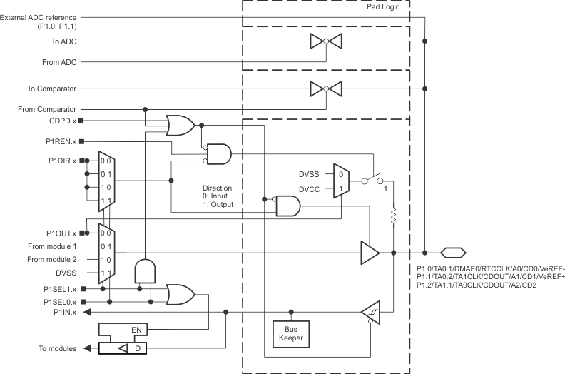
6.11.1 Port P1 (P1.0 to P1.2) Input/Output With Schmitt Trigger
Figure 6-9 shows the port diagram. Table 6-39 summarizes the selection of the pin functions.
Table 6-39 Port P1 (P1.0 to P1.2) Pin Functions
| PIN NAME (P1.x) | x | FUNCTION | CONTROL BITS OR SIGNALS | ||
|---|---|---|---|---|---|
| P1DIR.x | P1SEL1.x | P1SEL0.x | |||
| P1.0/TA0.1/DMAE0/RTCCLK/A0/CD0/VeREF- | 0 | P1.0 (I/O) | I: 0; O: 1 | 0 | 0 |
| TA0.CCI1A | 0 | 0 | 1 | ||
| TA0.1 | 1 | ||||
| DMAE0 | 0 | 1 | 0 | ||
| RTCCLK | 1 | ||||
| A0 (1) (3)
CD0 (1) (2) VeREF- (1) (3) |
X | 1 | 1 | ||
| P1.1/TA0.2/TA1CLK/CDOUT/A1/CD1/VeREF+ | 1 | P1.1 (I/O) | I: 0; O: 1 | 0 | 0 |
| TA0.CCI2A | 0 | 0 | 1 | ||
| TA0.2 | 1 | ||||
| TA1CLK | 0 | 1 | 0 | ||
| CDOUT | 1 | ||||
| A1 (1) (3)
CD1 (1) (2) VeREF+ (1) (3) |
X | 1 | 1 | ||
| P1.2/TA1.1/TA0CLK/CDOUT/A2/CD2 | 2 | P1.2 (I/O) | I: 0; O: 1 | 0 | 0 |
| TA1.CCI1A | 0 | 0 | 1 | ||
| TA1.1 | 1 | ||||
| TA0CLK | 0 | 1 | 0 | ||
| CDOUT | 1 | ||||
| A2 (1) (3)
CD2 (1) (2) |
X | 1 | 1 | ||
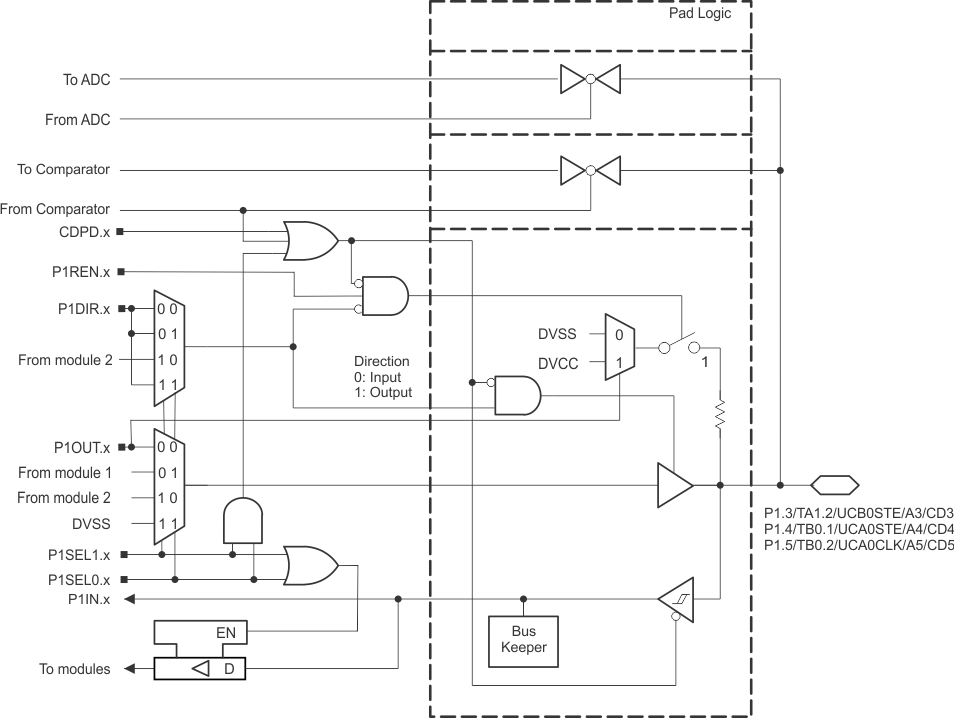
6.11.2 Port P1 (P1.3 to P1.5) Input/Output With Schmitt Trigger
Figure 6-10 shows the port diagram. Table 6-40 summarizes the selection of the pin functions.
Table 6-40 Port P1 (P1.3 to P1.5) Pin Functions
| PIN NAME (P1.x) | x | FUNCTION | CONTROL BITS OR SIGNALS | ||
|---|---|---|---|---|---|
| P1DIR.x | P1SEL1.x | P1SEL0.x | |||
| P1.3/TA1.2/UCB0STE/A3/CD3 | 3 | P1.3 (I/O) | I: 0; O: 1 | 0 | 0 |
| TA1.CCI2A | 0 | 0 | 1 | ||
| TA1.2 | 1 | ||||
| UCB0STE | X (1) | 1 | 0 | ||
| A3 (3) (5)
CD3 (3) (4) |
X | 1 | 1 | ||
| P1.4/TB0.1/UCA0STE/A4/CD4 | 4 | P1.4 (I/O) | I: 0; O: 1 | 0 | 0 |
| TB0.CCI1A | 0 | 0 | 1 | ||
| TB0.1 | 1 | ||||
| UCA0STE | X (2) | 1 | 0 | ||
| A4 (3) (5)
CD4 (3) (4) |
X | 1 | 1 | ||
| P1.5/TB0.2/UCA0CLK/A5/CD5 | 5 | P1.5(I/O) | I: 0; O: 1 | 0 | 0 |
| TB0.CCI2A | 0 | 0 | 1 | ||
| TB0.2 | 1 | ||||
| UCA0CLK | X (2) | 1 | 0 | ||
| A5 (3) (5)
CD5 (3) (4) |
X | 1 | 1 | ||
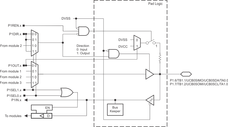
6.11.3 Port P1 (P1.6 and P1.7) Input/Output With Schmitt Trigger
Figure 6-11 shows the port diagram. Table 6-41 summarizes the selection of the pin functions.
Table 6-41 Port P1 (P1.6 and P1.7) Pin Functions
| PIN NAME (P1.x) | x | FUNCTION | CONTROL BITS OR SIGNALS | ||
|---|---|---|---|---|---|
| P1DIR.x | P1SEL1.x | P1SEL0.x | |||
| P1.6/TB1.1/UCB0SIMO/UCB0SDA/TA0.0 | 6 | P1.6 (I/O) | I: 0; O: 1 | 0 | 0 |
| TB1.CCI1A (2) | 0 | 0 | 1 | ||
| TB1.1 (2) | 1 | ||||
| UCB0SIMO/UCB0SDA | X (1) | 1 | 0 | ||
| TA0.CCI0A | 0 | 1 | 1 | ||
| TA0.0 | 1 | ||||
| P1.7/TB1.2/UCB0SOMI/UCB0SCL/TA1.0 | 7 | P1.7 (I/O) | I: 0; O: 1 | 0 | 0 |
| TB1.CCI2A (2) | 0 | 0 | 1 | ||
| TB1.2 (2) | 1 | ||||
| UCB0SOMI/UCB0SCL | X(1) | 1 | 0 | ||
| TA1.CCI0A | 0 | 1 | 1 | ||
| TA1.0 | 1 | ||||
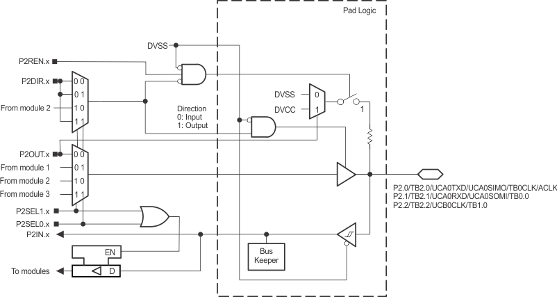
6.11.4 Port P2 (P2.0 to P2.2) Input/Output With Schmitt Trigger
Figure 6-12 shows the port diagram. Table 6-42 summarizes the selection of the pin functions.
Table 6-42 Port P2 (P2.0 to P2.2) Pin Functions
| PIN NAME (P2.x) | x | FUNCTION | CONTROL BITS OR SIGNALS | ||
|---|---|---|---|---|---|
| P2DIR.x | P2SEL1.x | P2SEL0.x | |||
| P2.0/TB2.0/UCA0TXD/UCA0SIMO/TB0CLK/ACLK | 0 | P2.0 (I/O) | I: 0; O: 1 | 0 | 0 |
| TB2.CCI0A (3) | 0 | 0 | 1 | ||
| TB2.0 (3) | 1 | ||||
| UCA0TXD/UCA0SIMO | X (1) | 1 | 0 | ||
| TB0CLK | 0 | 1 | 1 | ||
| ACLK | 1 | ||||
| P2.1/TB2.1/UCA0RXD/UCA0SOMI/TB0.0 | 1 | P2.1 (I/O) | I: 0; O: 1 | 0 | 0 |
| TB2.CCI1A (3) | 0 | 0 | 1 | ||
| TB2.1 (3) | 1 | ||||
| UCA0RXD/UCA0SOMI | X (1) | 1 | 0 | ||
| TB0.CCI0A | 0 | 1 | 1 | ||
| TB0.0 | 1 | ||||
| P2.2/TB2.2/UCB0CLK/TB1.0 | 2 | P2.2 (I/O) | I: 0; O: 1 | 0 | 0 |
| TB2.CCI2A (3) | 0 | 0 | 1 | ||
| TB2.2 (3) | 1 | ||||
| UCB0CLK | X (2) | 1 | 0 | ||
| TB1.CCI0A (3) | 0 | 1 | 1 | ||
| TB1.0 (3) | 1 | ||||
6.11.5 Port P2 (P2.3 and P2.4) Input/Output With Schmitt Trigger
Figure 6-13 shows the port diagram. Table 6-43 summarizes the selection of the pin functions.
Table 6-43 Port P2 (P2.3 and P2.4) Pin Functions
| PIN NAME (P2.x) | x | FUNCTION | CONTROL BITS OR SIGNALS | ||
|---|---|---|---|---|---|
| P2DIR.x | P2SEL1.x | P2SEL0.x | |||
| P2.3/TA0.0/UCA1STE/A6/CD10 | 3 | P2.3 (I/O) | I: 0; O: 1 | 0 | 0 |
| TA0.CCI0B | 0 | 0 | 1 | ||
| TA0.0 | 1 | ||||
| UCA1STE | X (1) | 1 | 0 | ||
| A6 (2) (4)
CD10 (2) (3) |
X | 1 | 1 | ||
| P2.4/TA1.0/UCA1CLK/A7/CD11 | 4 | P2.4 (I/O) | I: 0; O: 1 | 0 | 0 |
| TA1.CCI0B | 0 | 0 | 1 | ||
| TA1.0 | 1 | ||||
| UCA1CLK | X (1) | 1 | 0 | ||
| A7 (2) (4)
CD11 (2) (3) |
X | 1 | 1 | ||
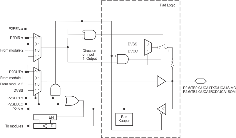
6.11.6 Port P2 (P2.5 and P2.6) Input/Output With Schmitt Trigger
Figure 6-14 shows the port diagram. Table 6-44 summarizes the selection of the pin functions.
Table 6-44 Port P2 (P2.5 and P2.6) Pin Functions
| PIN NAME (P2.x) | x | FUNCTION | CONTROL BITS OR SIGNALS | ||
|---|---|---|---|---|---|
| P2DIR.x | P2SEL1.x | P2SEL0.x | |||
| P2.5/TB0.0/UCA1TXD/UCA1SIMO | 5 | P2.5(I/O) (2) | I: 0; O: 1 | 0 | 0 |
| TB0.CCI0B (2) | 0 | 0 | 1 | ||
| TB0.0 (2) | 1 | ||||
| UCA1TXD/UCA1SIMO (2) | X (1) | 1 | 0 | ||
| P2.6/TB1.0/UCA1RXD/UCA1SOMI | 6 | P2.6(I/O) (2) | I: 0; O: 1 | 0 | 0 |
| TB1.CCI0B (2) | 0 | 0 | 1 | ||
| TB1.0 (2) | 1 | ||||
| UCA1RXD/UCA1SOMI (2) | X (1) | 1 | 0 | ||
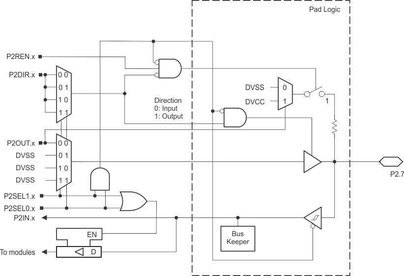
6.11.7 Port P2 (P2.7) Input/Output With Schmitt Trigger
Figure 6-15 shows the port diagram. Table 6-45 summarizes the selection of the pin functions.
Table 6-45 Port P2 (P2.7) Pin Functions
| PIN NAME (P2.x) | x | FUNCTION | CONTROL BITS OR SIGNALS | ||
|---|---|---|---|---|---|
| P2DIR.x | P2SEL1.x | P2SEL0.x | |||
| P2.7 | 7 | P2.7(I/O) (1) | I: 0; O: 1 | 0 | 0 |
6.11.8 Port P3 (P3.0 to P3.3) Input/Output With Schmitt Trigger
Figure 6-16 shows the port diagram. Table 6-46 summarizes the selection of the pin functions.
Table 6-46 Port P3 (P3.0 to P3.3) Pin Functions
| PIN NAME (P3.x) | x | FUNCTION | CONTROL BITS OR SIGNALS | ||
|---|---|---|---|---|---|
| P3DIR.x | P3SEL1.x | P3SEL0.x | |||
| P3.0/A12/CD12 | 0 | P3.0 (I/O) | I: 0; O: 1 | 0 | 0 |
| A12 (1) (3)
CD12 (1) (2) |
X | 1 | 1 | ||
| P3.1/A13/CD13 | 1 | P3.1 (I/O) | I: 0; O: 1 | 0 | 0 |
| A13 (1) (3)
CD13 (1) (2) |
X | 1 | 1 | ||
| P3.2/A14/CD14 | 2 | P3.2 (I/O) | I: 0; O: 1 | 0 | 0 |
| A14 (1) (3)
CD14 (1) (2) |
X | 1 | 1 | ||
| P3.3/A15/CD15 | 3 | P3.3 (I/O) | I: 0; O: 1 | 0 | 0 |
| A15 (1) (3)
CD15 (1) (2) |
X | 1 | 1 | ||
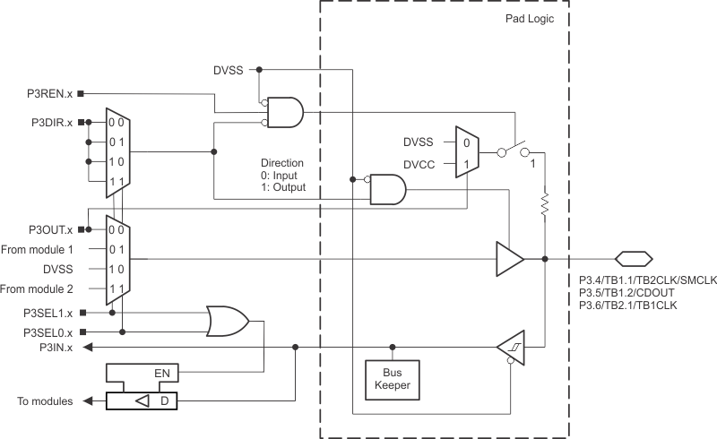
6.11.9 Port P3 (P3.4 to P3.6) Input/Output With Schmitt Trigger
Figure 6-17 shows the port diagram. Table 6-47 summarizes the selection of the pin functions.
Table 6-47 Port P3 (P3.4 to P3.6) Pin Functions
| PIN NAME (P3.x) | x | FUNCTION | CONTROL BITS OR SIGNALS | ||
|---|---|---|---|---|---|
| P3DIR.x | P3SEL1.x | P3SEL0.x | |||
| P3.4/TB1.1/TB2CLK/SMCLK | 4 | P3.4 (I/O) (1) | I: 0; O: 1 | 0 | 0 |
| TB1.CCI1B (1) | 0 | 0 | 1 | ||
| TB1.1 (1) | 1 | ||||
| TB2CLK (1) | 0 | 1 | 1 | ||
| SMCLK (1) | 1 | ||||
| P3.5/TB1.2/CDOUT | 5 | P3.5 (I/O) (1) | I: 0; O: 1 | 0 | 0 |
| TB1.CCI2B (1) | 0 | 0 | 1 | ||
| TB1.2 (1) | 1 | ||||
| CDOUT (1) | 1 | 1 | 1 | ||
| P3.6/TB2.1/TB1CLK | 6 | P3.6 (I/O) (1) | I: 0; O: 1 | 0 | 0 |
| TB2.CCI1B (1) | 0 | 0 | 1 | ||
| TB2.1 (1) | 1 | ||||
| TB1CLK (1) | 0 | 1 | 1 | ||
6.11.10 Port Port P3 (P3.7) Input/Output With Schmitt Trigger
Figure 6-18 shows the port diagram. Table 6-48 summarizes the selection of the pin functions.
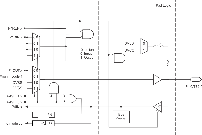
6.11.11 Port Port P4 (P4.0) Input/Output With Schmitt Trigger
Figure 6-19 shows the port diagram. Table 6-49 summarizes the selection of the pin functions.
6.11.12 Port Port P4 (P4.1) Input/Output With Schmitt Trigger
Figure 6-20 shows the port diagram. Table 6-50 summarizes the selection of the pin functions.
Table 6-50 Port P4 (P4.1) Pin Functions
| PIN NAME (P4.x) | x | FUNCTION | CONTROL BITS OR SIGNALS | ||
|---|---|---|---|---|---|
| P4DIR.x | P4SEL1.x | P4SEL0.x | |||
| P4.1 | 1 | P4.1 (I/O) (1) | I: 0; O: 1 | 0 | 0 |
6.11.13 Port Port PJ (PJ.0 to PJ.3) JTAG Pins TDO, TMS, TCK, TDI/TCLK, Input/Output With Schmitt Trigger or Output
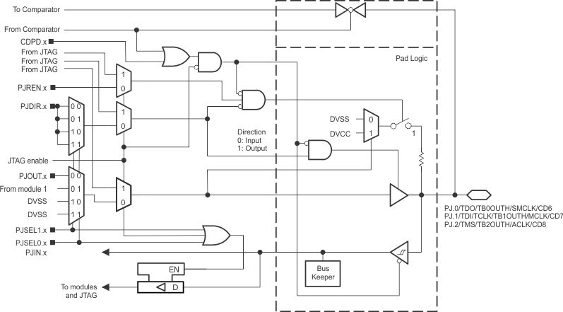
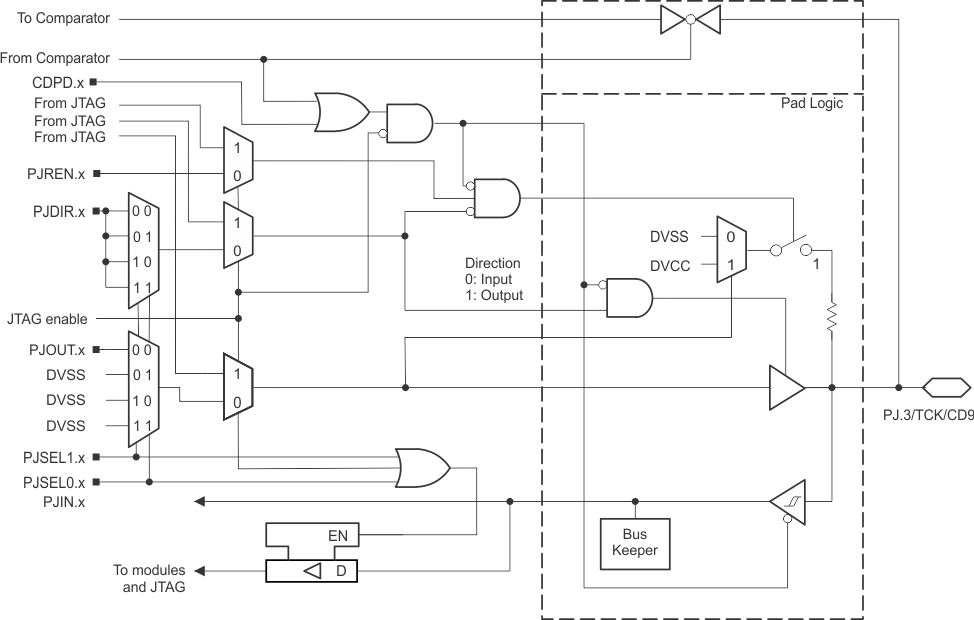
Figure 6-21 and Figure 6-22 show the port diagrams. Table 6-51 summarizes the selection of the pin functions.
Table 6-51 Port PJ (PJ.0 to PJ.3) Pin Functions
| PIN NAME (PJ.x) | x | FUNCTION | CONTROL BITS OR SIGNALS(1) | ||
|---|---|---|---|---|---|
| PJDIR.x | PJSEL1.x | PJSEL0.x | |||
| PJ.0/TDO/TB0OUTH/SMCLK/CD6 | 0 | PJ.0 (I/O) (2) | I: 0; O: 1 | 0 | 0 |
| TDO (3) | X | X | X | ||
| TB0OUTH | 0 | 0 | 1 | ||
| SMCLK | 1 | ||||
| CD6 | X | 1 | 1 | ||
| PJ.1/TDI/TCLK/TB1OUTH/MCLK/CD7 | 1 | PJ.1 (I/O) (2) | I: 0; O: 1 | 0 | 0 |
| TDI/TCLK (3) (4) | X | X | X | ||
| TB1OUTH | 0 | 0 | 1 | ||
| MCLK | 1 | ||||
| CD7 | X | 1 | 1 | ||
| PJ.2/TMS/TB2OUTH/ACLK/CD8 | 2 | PJ.2 (I/O) (2) | I: 0; O: 1 | 0 | 0 |
| TMS (3) (4) | X | X | X | ||
| TB2OUTH | 0 | 0 | 1 | ||
| ACLK | 1 | ||||
| CD8 | X | 1 | 1 | ||
| PJ.3/TCK/CD9 | 3 | PJ.3 (I/O) (2) | I: 0; O: 1 | 0 | 0 |
| TCK (3) (4) | X | X | X | ||
| CD9 | X | 1 | 1 | ||
6.11.14 Port Port PJ (PJ.4 and PJ.5) Input/Output With Schmitt Trigger
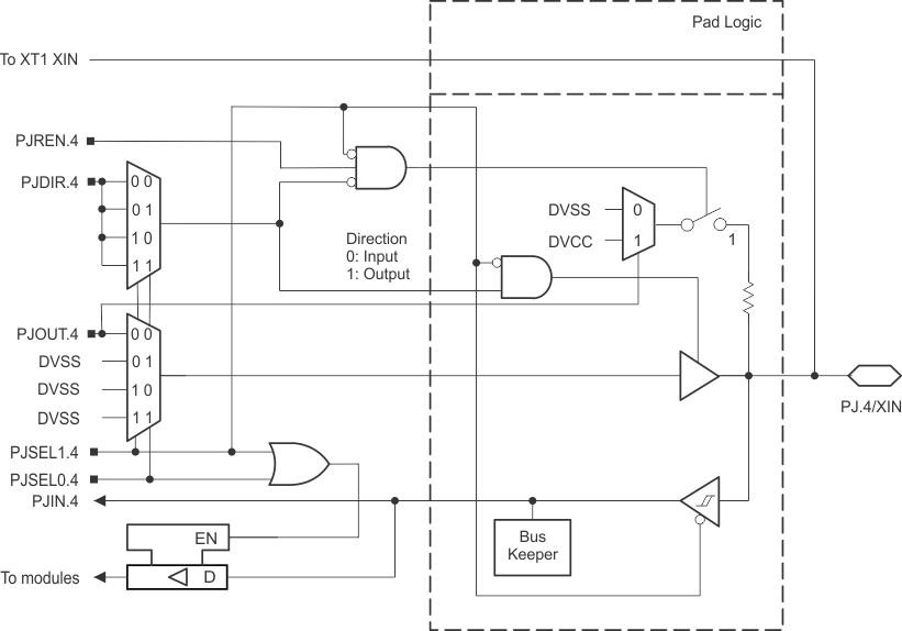
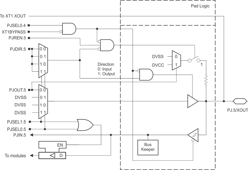
Figure 6-23 and Figure 6-24 show the port diagrams. Table 6-52 summarizes the selection of the pin functions.
Table 6-52 Port PJ (PJ.4 and PJ.5) Pin Functions
| PIN NAME (P7.x) | x | FUNCTION | CONTROL BITS OR SIGNALS (1) | |||||
|---|---|---|---|---|---|---|---|---|
| PJDIR.x | PJSEL1.5 | PJSEL0.5 | PJSEL1.4 | PJSEL0.4 | XT1 BYPASS | |||
| PJ.4/XIN | 4 | PJ.4 (I/O) | I: 0; O: 1 | X | X | 0 | 0 | X |
| XIN crystal mode (2) | X | X | X | 0 | 1 | 0 | ||
| XIN bypass mode (2) | X | X | X | 0 | 1 | 1 | ||
| PJ.5/XOUT | 5 | PJ.5 (I/O) | I: 0; O: 1 | 0 | 0 | 0 | 0 | X |
| XOUT crystal mode (2) | X | X | X | 0 | 1 | 0 | ||
| PJ.5 (I/O) (3) | I: 0; O: 1 | X | X | 0 | 1 | 1 | ||
6.12 Device Descriptors (TLV)
Table 6-53 and Table 6-54 list the complete contents of the device descriptor tag-length-value (TLV) structure for each device type.
Table 6-53 Device Descriptor Table (1)
| DESCRIPTION | ADDRESS | VALUE | |||||
|---|---|---|---|---|---|---|---|
| FR5739 | FR5738 | FR5737 | FR5736 | FR5735 | |||
| Info Block | Info length | 01A00h | 05h | 05h | 05h | 05h | 05h |
| CRC length | 01A01h | 05h | 05h | 05h | 05h | 05h | |
| CRC value | 01A02h | per unit | per unit | per unit | per unit | per unit | |
| 01A03h | per unit | per unit | per unit | per unit | per unit | ||
| Device ID | 01A04h | 03h | 02h | 01h | 77h | 76h | |
| Device ID | 01A05h | 81h | 81h | 81h | 81h | 81h | |
| Hardware revision | 01A06h | per unit | per unit | per unit | per unit | per unit | |
| Firmware revision | 01A07h | per unit | per unit | per unit | per unit | per unit | |
| Die Record | Die record tag | 01A08h | 08h | 08h | 08h | 08h | 08h |
| Die record length | 01A09h | 0Ah | 0Ah | 0Ah | 0Ah | 0Ah | |
| Lot/wafer ID | 01A0Ah | per unit | per unit | per unit | per unit | per unit | |
| 01A0Bh | per unit | per unit | per unit | per unit | per unit | ||
| 01A0Ch | per unit | per unit | per unit | per unit | per unit | ||
| 01A0Dh | per unit | per unit | per unit | per unit | per unit | ||
| Die X position | 01A0Eh | per unit | per unit | per unit | per unit | per unit | |
| 01A0Fh | per unit | per unit | per unit | per unit | per unit | ||
| Die Y position | 01A10h | per unit | per unit | per unit | per unit | per unit | |
| 01A11h | per unit | per unit | per unit | per unit | per unit | ||
| Test results | 01A12h | per unit | per unit | per unit | per unit | per unit | |
| 01A13h | per unit | per unit | per unit | per unit | per unit | ||
| ADC10 Calibration | ADC10 calibration tag | 01A14h | 13h | 13h | 13h | 05h | 13h |
| ADC10 calibration length | 01A15h | 10h | 10h | 10h | 10h | 10h | |
| ADC gain factor | 01A16h | per unit | per unit | NA | NA | per unit | |
| 01A17h | per unit | per unit | NA | NA | per unit | ||
| ADC offset | 01A18h | per unit | per unit | NA | NA | per unit | |
| 01A19h | per unit | per unit | NA | NA | per unit | ||
| ADC 1.5-V reference Temp. sensor 30°C |
01A1Ah | per unit | per unit | NA | NA | per unit | |
| 01A1Bh | per unit | per unit | NA | NA | per unit | ||
| ADC 1.5-V reference Temp. sensor 85°C |
01A1Ch | per unit | per unit | NA | NA | per unit | |
| 01A1Dh | per unit | per unit | NA | NA | per unit | ||
| ADC 2.0-V reference Temp. sensor 30°C |
01A1Eh | per unit | per unit | NA | NA | per unit | |
| 01A1Fh | per unit | per unit | NA | NA | per unit | ||
| ADC 2.0-V reference Temp. sensor 85°C |
01A20h | per unit | per unit | NA | NA | per unit | |
| 01A21h | per unit | per unit | NA | NA | per unit | ||
| ADC 2.5-V reference Temp. sensor 30°C |
01A22h | per unit | per unit | NA | NA | per unit | |
| 01A23h | per unit | per unit | NA | NA | per unit | ||
| ADC 2.5-V reference Temp. sensor 85°C |
01A24h | per unit | per unit | NA | NA | per unit | |
| 01A25h | per unit | per unit | NA | NA | per unit | ||
| REF Calibration | REF calibration tag | 01A26h | 12h | 12h | 12h | 12h | 12h |
| REF calibration length | 01A27h | 06h | 06h | 06h | 06h | 06h | |
| REF 1.5-V reference | 01A28h | per unit | per unit | per unit | per unit | per unit | |
| 01A29h | per unit | per unit | per unit | per unit | per unit | ||
| REF 2.0-V reference | 01A2Ah | per unit | per unit | per unit | per unit | per unit | |
| 01A2Bh | per unit | per unit | per unit | per unit | per unit | ||
| REF 2.5-V reference | 01A2Ch | per unit | per unit | per unit | per unit | per unit | |
| 01A2Dh | per unit | per unit | per unit | per unit | per unit | ||
Table 6-54 Device Descriptor Table (1)
| DESCRIPTION | ADDRESS | VALUE | |||||
|---|---|---|---|---|---|---|---|
| FR5734 | FR5733 | FR5732 | FR5731 | FR5730 | |||
| Info Block | Info length | 01A00h | 05h | 05h | 05h | 05h | 05h |
| CRC length | 01A01h | 05h | 05h | 05h | 05h | 05h | |
| CRC value | 01A02h | per unit | per unit | per unit | per unit | per unit | |
| 01A03h | per unit | per unit | per unit | per unit | per unit | ||
| Device ID | 01A04h | 00h | 7Fh | 75h | 7Eh | 7Ch | |
| Device ID | 01A05h | 81h | 80h | 81h | 80h | 80h | |
| Hardware revision | 01A06h | per unit | per unit | per unit | per unit | per unit | |
| Firmware revision | 01A07h | per unit | per unit | per unit | per unit | per unit | |
| Die Record | Die record tag | 01A08h | 08h | 08h | 08h | 08h | 08h |
| Die record length | 01A09h | 0Ah | 0Ah | 0Ah | 0Ah | 0Ah | |
| Lot/wafer ID | 01A0Ah | per unit | per unit | per unit | per unit | per unit | |
| 01A0Bh | per unit | per unit | per unit | per unit | per unit | ||
| 01A0Ch | per unit | per unit | per unit | per unit | per unit | ||
| 01A0Dh | per unit | per unit | per unit | per unit | per unit | ||
| Die X position | 01A0Eh | per unit | per unit | per unit | per unit | per unit | |
| 01A0Fh | per unit | per unit | per unit | per unit | per unit | ||
| Die Y position | 01A10h | per unit | per unit | per unit | per unit | per unit | |
| 01A11h | per unit | per unit | per unit | per unit | per unit | ||
| Test results | 01A12h | per unit | per unit | per unit | per unit | per unit | |
| 01A13h | per unit | per unit | per unit | per unit | per unit | ||
| ADC10 Calibration | ADC10 calibration tag | 01A14h | 13h | 13h | 13h | 05h | 13h |
| ADC10 calibration length | 01A15h | 10h | 10h | 10h | 10h | 10h | |
| ADC gain factor | 01A16h | per unit | NA | NA | per unit | per unit | |
| 01A17h | per unit | NA | NA | per unit | per unit | ||
| ADC Offset | 01A18h | per unit | NA | NA | per unit | per unit | |
| 01A19h | per unit | NA | NA | per unit | per unit | ||
| ADC 1.5-V reference Temp. sensor 30°C |
01A1Ah | per unit | NA | NA | per unit | per unit | |
| 01A1Bh | per unit | NA | NA | per unit | per unit | ||
| ADC 1.5-V reference Temp. sensor 85°C |
01A1Ch | per unit | NA | NA | per unit | per unit | |
| 01A1Dh | per unit | NA | NA | per unit | per unit | ||
| ADC 2.0-V reference Temp. sensor 30°C |
01A1Eh | per unit | NA | NA | per unit | per unit | |
| 01A1Fh | per unit | NA | NA | per unit | per unit | ||
| ADC 2.0-V reference Temp. sensor 85°C |
01A20h | per unit | NA | NA | per unit | per unit | |
| 01A21h | per unit | NA | NA | per unit | per unit | ||
| ADC 2.5-V reference Temp. sensor 30°C |
01A22h | per unit | NA | NA | per unit | per unit | |
| 01A23h | per unit | NA | NA | per unit | per unit | ||
| ADC 2.5-V reference Temp. sensor 85°C |
01A24h | per unit | NA | NA | per unit | per unit | |
| 01A25h | per unit | NA | NA | per unit | per unit | ||
| REF Calibration | REF calibration tag | 01A26h | 12h | 12h | 12h | 12h | 12h |
| REF Calibration length | 01A27h | 06h | 06h | 06h | 06h | 06h | |
| REF 1.5-V reference | 01A28h | per unit | per unit | per unit | per unit | per unit | |
| 01A29h | per unit | per unit | per unit | per unit | per unit | ||
| REF 2.0-V reference | 01A2Ah | per unit | per unit | per unit | per unit | per unit | |
| 01A2Bh | per unit | per unit | per unit | per unit | per unit | ||
| REF 2.5-V reference | 01A2Ch | per unit | per unit | per unit | per unit | per unit | |
| 01A2Dh | per unit | per unit | per unit | per unit | per unit | ||
