SLVSCN6A November 2014 – December 2014 MSP430FR5739-EP
PRODUCTION DATA.
- 1Device Overview
- 2Revision History
- 3Pin Configuration and Functions
-
4Specifications
- 4.1 Absolute Maximum Ratings
- 4.2 Recommended Operating Conditions
- 4.3 Thermal Information
- 4.4 Active Mode Supply Current Into VCC Excluding External Current
- 4.5 Low-Power Mode Supply Currents (Into VCC) Excluding External Current
- 4.6 Schmitt-Trigger Inputs - General Purpose I/O (P1.0 to P1.7, P2.0 to P2.7, P3.0 to P3.7, P4.0 to P4.1, PJ.0 to PJ.5, RST/NMI)
- 4.7 Inputs - Ports P1 and P2 (P1.0 to P1.7, P2.0 to P2.7)
- 4.8 Leakage Current - General Purpose I/O (P1.0 to P1.7, P2.0 to P2.7, P3.0 to P3.7, P4.0 to P4.1, PJ.0 to PJ.5, RST/NMI)
- 4.9 Outputs - General Purpose I/O (P1.0 to P1.7, P2.0 to P2.7, P3.0 to P3.7, P4.0 to P4.1, PJ.0 to PJ.5)
- 4.10 Output Frequency - General Purpose I/O (P1.0 to P1.7, P2.0 to P2.7, P3.0 to P3.7, P4.0 to P4.1, PJ.0 to PJ.5)
- 4.11 Typical Characteristics - Outputs
- 4.12 Crystal Oscillator, XT1, Low-Frequency (LF) Mode
- 4.13 Crystal Oscillator, XT1, High-Frequency (HF) Mode
- 4.14 Internal Very-Low-Power Low-Frequency Oscillator (VLO)
- 4.15 DCO Frequencies
- 4.16 MODOSC
- 4.17 PMM, Core Voltage
- 4.18 PMM, SVS, BOR
- 4.19 Wake-Up from Low Power Modes
- 4.20 Timer_A
- 4.21 Timer_B
- 4.22 eUSCI (UART Mode) Recommended Operating Conditions
- 4.23 eUSCI (UART Mode)
- 4.24 eUSCI (SPI Master Mode) Recommended Operating Conditions
- 4.25 eUSCI (SPI Master Mode)
- 4.26 eUSCI (SPI Slave Mode)
- 4.27 eUSCI (I2C Mode)
- 4.28 10-Bit ADC, Power Supply and Input Range Conditions
- 4.29 10-Bit ADC, Timing Parameters
- 4.30 10-Bit ADC, Linearity Parameters
- 4.31 REF, External Reference
- 4.32 REF, Built-In Reference
- 4.33 REF, Temperature Sensor and Built-In VMID
- 4.34 Comparator_D
- 4.35 FRAM
- 4.36 JTAG and Spy-Bi-Wire Interface
-
5Detailed Description
- 5.1 Functional Block Diagram
- 5.2 CPU
- 5.3 Operating Modes
- 5.4 Interrupt Vector Addresses
- 5.5 Memory Organization
- 5.6 Bootstrap Loader (BSL)
- 5.7 JTAG Operation
- 5.8 FRAM
- 5.9 Memory Protection Unit (MPU)
- 5.10
Peripherals
- 5.10.1 Digital I/O
- 5.10.2 Oscillator and Clock System (CS)
- 5.10.3 Power Management Module (PMM)
- 5.10.4 Hardware Multiplier (MPY)
- 5.10.5 Real-Time Clock (RTC_B)
- 5.10.6 Watchdog Timer (WDT_A)
- 5.10.7 System Module (SYS)
- 5.10.8 DMA Controller
- 5.10.9 Enhanced Universal Serial Communication Interface (eUSCI)
- 5.10.10 TA0, TA1
- 5.10.11 TB0, TB1, TB2
- 5.10.12 ADC10_B
- 5.10.13 Comparator_D
- 5.10.14 CRC16
- 5.10.15 Shared Reference (REF)
- 5.10.16 Embedded Emulation Module (EEM)
- 5.10.17 Peripheral File Map
-
6Input/Output Schematics
- 6.1 Port P1, P1.0 to P1.2, Input/Output With Schmitt Trigger
- 6.2 Port P1, P1.3 to P1.5, Input/Output With Schmitt Trigger
- 6.3 Port P1, P1.6 to P1.7, Input/Output With Schmitt Trigger
- 6.4 Port P2, P2.0 to P2.2, Input/Output With Schmitt Trigger
- 6.5 Port P2, P2.3 to P2.4, Input/Output With Schmitt Trigger
- 6.6 Port P2, P2.5 to P2.6, Input/Output With Schmitt Trigger
- 6.7 Port P2, P2.7, Input/Output With Schmitt Trigger
- 6.8 Port P3, P3.0 to P3.3, Input/Output With Schmitt Trigger
- 6.9 Port P3, P3.4 to P3.6, Input/Output With Schmitt Trigger
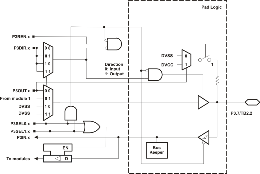
- 6.10 Port P3, P3.7, Input/Output With Schmitt Trigger
- 6.11 Port P4, P4.0, Input/Output With Schmitt Trigger
- 6.12 Port P4, P4.1, Input/Output With Schmitt Trigger
- 6.13 Port J, J.0 to J.3 JTAG pins TDO, TMS, TCK, TDI/TCLK, Input/Output With Schmitt Trigger or Output
- 6.14 Port PJ, PJ.4 and PJ.5 Input/Output With Schmitt Trigger
- 7Device Descriptors (TLV)
-
8Device and Documentation Support
- 8.1 Device Support
- 8.2 Documentation Support
- 8.3 Community Resources
- 8.4 Trademarks
- 8.5 Electrostatic Discharge Caution
- 8.6 Glossary
- 9Mechanical Packaging and Orderable Information
Package Options
Mechanical Data (Package|Pins)
- RHA|40
Thermal pad, mechanical data (Package|Pins)
- RHA|40
Orderable Information
6 Input/Output Schematics
6.1 Port P1, P1.0 to P1.2, Input/Output With Schmitt Trigger
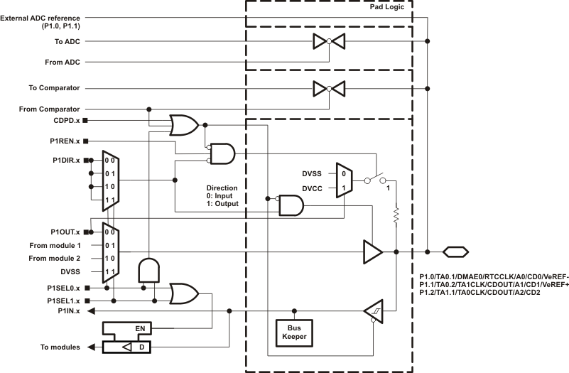
Table 6-1 Port P1 (P1.0 to P1.2) Pin Functions
| PIN NAME (P1.x) | x | FUNCTION | CONTROL BITS/SIGNALS | ||
|---|---|---|---|---|---|
| P1DIR.x | P1SEL1.x | P1SEL0.x | |||
| P1.0/TA0.1/DMAE0/RTCCLK/A0/CD0/VeREF- | 0 | P1.0 (I/O) | I: 0; O: 1 | 0 | 0 |
| TA0.CCI1A | 0 | 0 | 1 | ||
| TA0.1 | 1 | ||||
| DMAE0 | 0 | 1 | 0 | ||
| RTCCLK | 1 | ||||
| A0 (1)(3)
CD0 (1)(2) VeREF- (1)(3) |
X | 1 | 1 | ||
| P1.1/TA0.2/TA1CLK/CDOUT/A1/CD1/VeREF+ | 1 | P1.1 (I/O) | I: 0; O: 1 | 0 | 0 |
| TA0.CCI2A | 0 | 0 | 1 | ||
| TA0.2 | 1 | ||||
| TA1CLK | 0 | 1 | 0 | ||
| CDOUT | 1 | ||||
| A1 (1)(3)
CD1 (1)(2) VeREF+ (1)(3) |
X | 1 | 1 | ||
| P1.2/TA1.1/TA0CLK/CDOUT/A2/CD2 | 2 | P1.2 (I/O) | I: 0; O: 1 | 0 | 0 |
| TA1.CCI1A | 0 | 0 | 1 | ||
| TA1.1 | 1 | ||||
| TA0CLK | 0 | 1 | 0 | ||
| CDOUT | 1 | ||||
| A2 (1)(3)
CD2 (1)(2) |
X | 1 | 1 | ||
(1) Setting P1SEL1.x and P1SEL0.x disables the output driver as well as the input Schmitt trigger to prevent parasitic cross currents when applying analog signals.
(2) Setting the CDPD.x bit of the comparator disables the output driver as well as the input Schmitt trigger to prevent parasitic cross currents when applying analog signals. Selecting the CDx input pin to the comparator multiplexer with the CDx bits automatically disables output driver and input buffer for that pin, regardless of the state of the associated CDPD.x bit.
(3) Not available on all devices and package types.
6.2 Port P1, P1.3 to P1.5, Input/Output With Schmitt Trigger
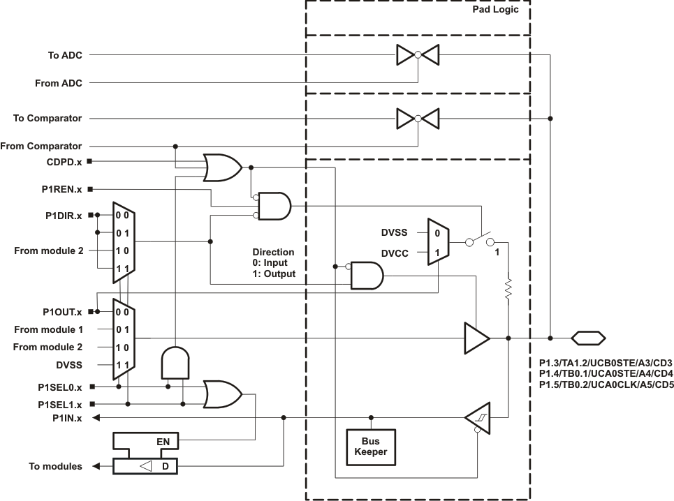
Table 6-2 Port P1 (P1.3 to P1.5) Pin Functions
| PIN NAME (P1.x) | x | FUNCTION | CONTROL BITS/SIGNALS | ||
|---|---|---|---|---|---|
| P1DIR.x | P1SEL1.x | P1SEL0.x | |||
| P1.3/TA1.2/UCB0STE/A3/CD3 | 3 | P1.3 (I/O) | I: 0; O: 1 | 0 | 0 |
| TA1.CCI2A | 0 | 0 | 1 | ||
| TA1.2 | 1 | ||||
| UCB0STE | X (1) | 1 | 0 | ||
| A3 (3)(5)
CD3 (3)(4) |
X | 1 | 1 | ||
| P1.4/TB0.1/UCA0STE/A4/CD4 | 4 | P1.4 (I/O) | I: 0; O: 1 | 0 | 0 |
| TB0.CCI1A | 0 | 0 | 1 | ||
| TB0.1 | 1 | ||||
| UCA0STE | X (2) | 1 | 0 | ||
| A4 (3)(5)
CD4 (3)(4) |
X | 1 | 1 | ||
| P1.5/TB0.2/UCA0CLK/A5/CD5 | 5 | P1.5(I/O) | I: 0; O: 1 | 0 | 0 |
| TB0.CCI2A | 0 | 0 | 1 | ||
| TB0.2 | 1 | ||||
| UCA0CLK | X (2) | 1 | 0 | ||
| A5 (3)(5)
CD5 (3)(4) |
X | 1 | 1 | ||
(1) Direction controlled by eUSCI_B0 module.
(2) Direction controlled by eUSCI_A0 module.
(3) Setting P1SEL1.x and P1SEL0.x disables the output driver and the input Schmitt trigger to prevent parasitic cross currents when applying analog signals.
(4) Setting the CDPD.x bit of the comparator disables the output driver and the input Schmitt trigger to prevent parasitic cross currents when applying analog signals. Selecting the CDx input pin to the comparator multiplexer with the CDx bits automatically disables output driver and input buffer for that pin, regardless of the state of the associated CDPD.x bit
(5) Not available on all devices and package types.
6.3 Port P1, P1.6 to P1.7, Input/Output With Schmitt Trigger
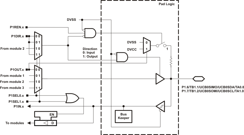
Table 6-3 Port P1 (P1.6 to P1.7) Pin Functions
| PIN NAME (P1.x) | x | FUNCTION | CONTROL BITS/SIGNALS | ||
|---|---|---|---|---|---|
| P1DIR.x | P1SEL1.x | P1SEL0.x | |||
| P1.6/TB1.1/UCB0SIMO/UCB0SDA/TA0.0 | 6 | P1.6 (I/O) | I: 0; O: 1 | 0 | 0 |
| TB1.CCI1A (2) | 0 | 0 | 1 | ||
| TB1.1 (2) | 1 | ||||
| UCB0SIMO/UCB0SDA | X (1) | 1 | 0 | ||
| TA0.CCI0A | 0 | 1 | 1 | ||
| TA0.0 | 1 | ||||
| P1.7/TB1.2/UCB0SOMI/UCB0SCL/TA1.0 | 7 | P1.7 (I/O) | I: 0; O: 1 | 0 | 0 |
| TB1.CCI2A (2) | 0 | 0 | 1 | ||
| TB1.2 (2) | 1 | ||||
| UCB0SOMI/UCB0SCL | X(1) | 1 | 0 | ||
| TA1.CCI0A | 0 | 1 | 1 | ||
| TA1.0 | 1 | ||||
(1) Direction controlled by eUSCI_B0 module.
(2) Not available on all devices and package types.
6.4 Port P2, P2.0 to P2.2, Input/Output With Schmitt Trigger
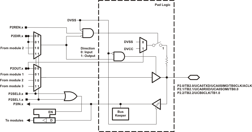
Table 6-4 Port P2 (P2.0 to P2.2) Pin Functions
| PIN NAME (P2.x) | x | FUNCTION | CONTROL BITS/SIGNALS | ||
|---|---|---|---|---|---|
| P2DIR.x | P2SEL1.x | P2SEL0.x | |||
| P2.0/TB2.0/UCA0TXD/UCA0SIMO/TB0CLK/ACLK | 0 | P2.0 (I/O) | I: 0; O: 1 | 0 | 0 |
| TB2.CCI0A (3) | 0 | 0 | 1 | ||
| TB2.0 (3) | 1 | ||||
| UCA0TXD/UCA0SIMO | X (1) | 1 | 0 | ||
| TB0CLK | 0 | 1 | 1 | ||
| ACLK | 1 | ||||
| P2.1/TB2.1/UCA0RXD/UCA0SOMI/TB0.0 | 1 | P2.1 (I/O) | I: 0; O: 1 | 0 | 0 |
| TB2.CCI1A (3) | 0 | 0 | 1 | ||
| TB2.1 (3) | 1 | ||||
| UCA0RXD/UCA0SOMI | X (1) | 1 | 0 | ||
| TB0.CCI0A | 0 | 1 | 1 | ||
| TB0.0 | 1 | ||||
| P2.2/TB2.2/UCB0CLK/TB1.0 | 2 | P2.2 (I/O) | I: 0; O: 1 | 0 | 0 |
| TB2.CCI2A (3) | 0 | 0 | 1 | ||
| TB2.2 (3) | 1 | ||||
| UCB0CLK | X (2) | 1 | 0 | ||
| TB1.CCI0A (3) | 0 | 1 | 1 | ||
| TB1.0 (3) | 1 | ||||
(1) Direction controlled by eUSCI_A0 module.
(2) Direction controlled by eUSCI_B0 module.
(3) Not available on all devices and package types.
6.5 Port P2, P2.3 to P2.4, Input/Output With Schmitt Trigger
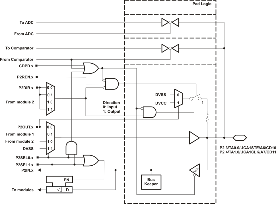
Table 6-5 Port P2 (P2.3 to P2.4) Pin Functions
| PIN NAME (P2.x) | x | FUNCTION | CONTROL BITS/SIGNALS | ||
|---|---|---|---|---|---|
| P2DIR.x | P2SEL1.x | P2SEL0.x | |||
| P2.3/TA0.0/UCA1STE/A6/CD10 | 3 | P2.3 (I/O) | I: 0; O: 1 | 0 | 0 |
| TA0.CCI0B | 0 | 0 | 1 | ||
| TA0.0 | 1 | ||||
| UCA1STE | X (1) | 1 | 0 | ||
| A6 (2)(4)
CD10 (2)(3) |
X | 1 | 1 | ||
| P2.4/TA1.0/UCA1CLK/A7/CD11 | 4 | P2.4 (I/O) | I: 0; O: 1 | 0 | 0 |
| TA1.CCI0B | 0 | 0 | 1 | ||
| TA1.0 | 1 | ||||
| UCA1CLK | X (1) | 1 | 0 | ||
| A7 (2)(4)
CD11 (2)(3) |
X | 1 | 1 | ||
(1) Direction controlled by eUSCI_A1 module.
(2) Setting P2SEL1.x and P2SEL0.x disables the output driver and the input Schmitt trigger to prevent parasitic cross currents when applying analog signals.
(3) Setting the CDPD.x bit of the comparator disables the output driver and the input Schmitt trigger to prevent parasitic cross currents when applying analog signals. Selecting the CDx input pin to the comparator multiplexer with the CDx bits automatically disables output driver and input buffer for that pin, regardless of the state of the associated CDPD.x bit.
(4) Not available on all devices and package types.
6.6 Port P2, P2.5 to P2.6, Input/Output With Schmitt Trigger
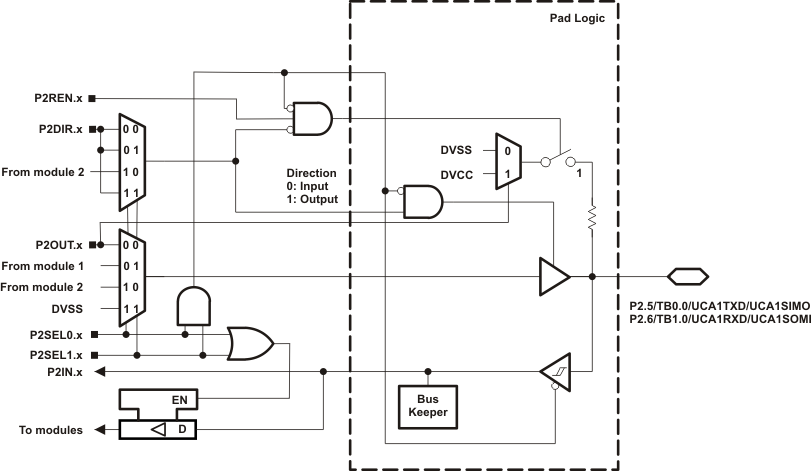
Table 6-6 Port P2 (P2.5 to P2.6) Pin Functions
| PIN NAME (P2.x) | x | FUNCTION | CONTROL BITS/SIGNALS | ||
|---|---|---|---|---|---|
| P2DIR.x | P2SEL1.x | P2SEL0.x | |||
| P2.5/TB0.0/UCA1TXD/UCA1SIMO | 5 | P2.5(I/O) (2) | I: 0; O: 1 | 0 | 0 |
| TB0.CCI0B (2) | 0 | 0 | 1 | ||
| TB0.0 (2) | 1 | ||||
| UCA1TXD/UCA1SIMO (2) | X (1) | 1 | 0 | ||
| P2.6/TB1.0/UCA1RXD/UCA1SOMI | 6 | P2.6(I/O) (2) | I: 0; O: 1 | 0 | 0 |
| TB1.CCI0B (2) | 0 | 0 | 1 | ||
| TB1.0 (2) | 1 | ||||
| UCA1RXD/UCA1SOMI (2) | X (1) | 1 | 0 | ||
(1) Direction controlled by eUSCI_A1 module.
(2) Not available on all devices and package types.
6.7 Port P2, P2.7, Input/Output With Schmitt Trigger
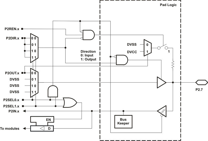
Table 6-7 Port P2 (P2.7) Pin Functions
| PIN NAME (P2.x) | x | FUNCTION | CONTROL BITS/SIGNALS | ||
|---|---|---|---|---|---|
| P2DIR.x | P2SEL1.x | P2SEL0.x | |||
| P2.7 | 7 | P2.7(I/O) (1) | I: 0; O: 1 | 0 | 0 |
(1) Not available on all devices and package types.
6.8 Port P3, P3.0 to P3.3, Input/Output With Schmitt Trigger
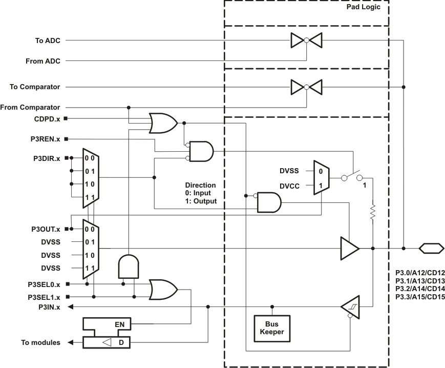
Table 6-8 Port P3 (P3.0 to P3.3) Pin Functions
| PIN NAME (P3.x) | x | FUNCTION | CONTROL BITS/SIGNALS | ||
|---|---|---|---|---|---|
| P3DIR.x | P3SEL1.x | P3SEL0.x | |||
| P3.0/A12/CD12 | 0 | P3.0 (I/O) | I: 0; O: 1 | 0 | 0 |
| A12 (1)(3)
CD12 (1)(2) |
X | 1 | 1 | ||
| P3.1/A13/CD13 | 1 | P3.1 (I/O) | I: 0; O: 1 | 0 | 0 |
| A13 (1)(3)
CD13 (1)(2) |
X | 1 | 1 | ||
| P3.2/A14/CD14 | 2 | P3.2 (I/O) | I: 0; O: 1 | 0 | 0 |
| A14 (1)(3)
CD14 (1)(2) |
X | 1 | 1 | ||
| P3.3/A15/CD15 | 3 | P3.3 (I/O) | I: 0; O: 1 | 0 | 0 |
| A15 (1)(3)
CD15 (1)(2) |
X | 1 | 1 | ||
(1) Setting P1SEL1.x and P1SEL0.x disables the output driver and the input Schmitt trigger to prevent parasitic cross currents when applying analog signals.
(2) Setting the CDPD.x bit of the comparator disables the output driver and the input Schmitt trigger to prevent parasitic cross currents when applying analog signals. Selecting the CDx input pin to the comparator multiplexer with the CDx bits automatically disables output driver and input buffer for that pin, regardless of the state of the associated CDPD.x bit.
(3) Not available on all devices and package types.
6.9 Port P3, P3.4 to P3.6, Input/Output With Schmitt Trigger
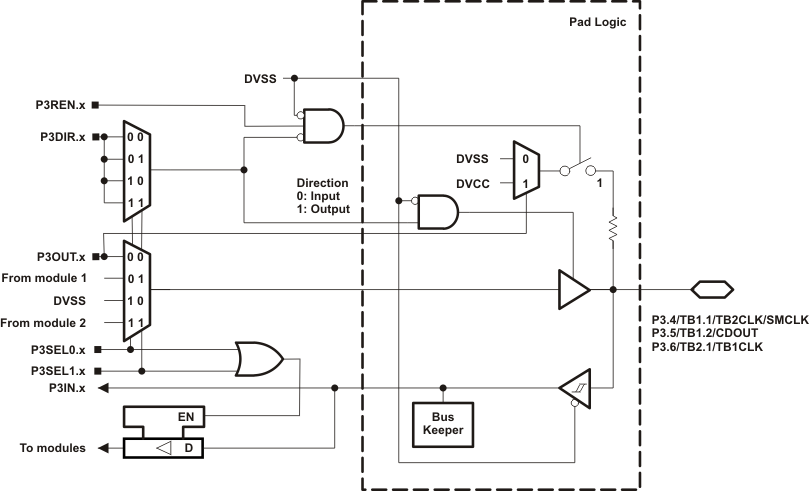
Table 6-9 Port P3 (P3.4 to P3.6) Pin Functions
| PIN NAME (P3.x) | x | FUNCTION | CONTROL BITS/SIGNALS | ||
|---|---|---|---|---|---|
| P3DIR.x | P3SEL1.x | P3SEL0.x | |||
| P3.4/TB1.1/TB2CLK/SMCLK | 4 | P3.4 (I/O) (1) | I: 0; O: 1 | 0 | 0 |
| TB1.CCI1B (1) | 0 | 0 | 1 | ||
| TB1.1 (1) | 1 | ||||
| TB2CLK (1) | 0 | 1 | 1 | ||
| SMCLK (1) | 1 | ||||
| P3.5/TB1.2/CDOUT | 5 | P3.5 (I/O) (1) | I: 0; O: 1 | 0 | 0 |
| TB1.CCI2B (1) | 0 | 0 | 1 | ||
| TB1.2 (1) | 1 | ||||
| CDOUT (1) | 1 | 1 | 1 | ||
| P3.6/TB2.1/TB1CLK | 6 | P3.6 (I/O) (1) | I: 0; O: 1 | 0 | 0 |
| TB2.CCI1B (1) | 0 | 0 | 1 | ||
| TB2.1 (1) | 1 | ||||
| TB1CLK (1) | 0 | 1 | 1 | ||
(1) Not available on all devices and package types.
6.10 Port P3, P3.7, Input/Output With Schmitt Trigger
6.11 Port P4, P4.0, Input/Output With Schmitt Trigger

6.12 Port P4, P4.1, Input/Output With Schmitt Trigger

Table 6-12 Port P4 (P4.1) Pin Functions
| PIN NAME (P4.x) | x | FUNCTION | CONTROL BITS/SIGNALS | ||
|---|---|---|---|---|---|
| P4DIR.x | P4SEL1.x | P4SEL0.x | |||
| P4.1 | 1 | P4.1 (I/O) (1) | I: 0; O: 1 | 0 | 0 |
(1) Not available on all devices and package types.
6.13 Port J, J.0 to J.3 JTAG pins TDO, TMS, TCK, TDI/TCLK, Input/Output With Schmitt Trigger or Output
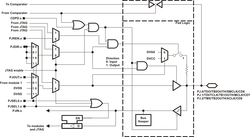
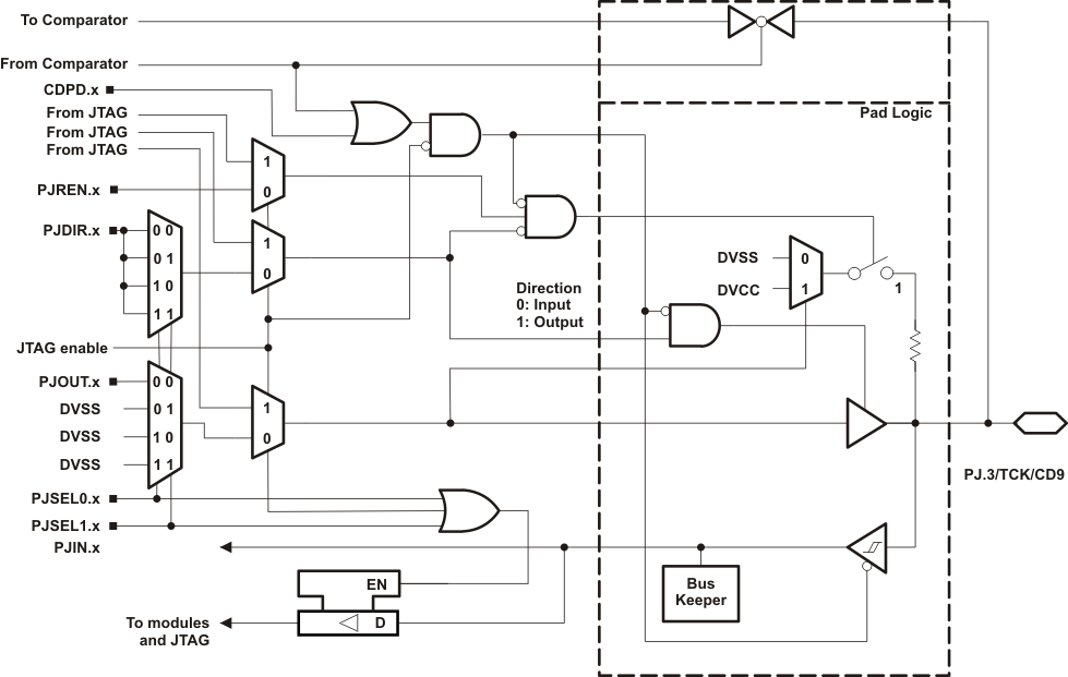
Table 6-13 Port PJ (PJ.0 to PJ.3) Pin Functions
| PIN NAME (PJ.x) | x | FUNCTION | CONTROL BITS/ SIGNALS (1) | ||
|---|---|---|---|---|---|
| PJDIR.x | PJSEL1.x | PJSEL0.x | |||
| PJ.0/TDO/TB0OUTH/SMCLK/CD6 | 0 | PJ.0 (I/O) (2) | I: 0; O: 1 | 0 | 0 |
| TDO (3) | X | X | X | ||
| TB0OUTH | 0 | 0 | 1 | ||
| SMCLK | 1 | ||||
| CD6 | X | 1 | 1 | ||
| PJ.1/TDI/TCLK/TB1OUTH/MCLK/CD7 | 1 | PJ.1 (I/O) (2) | I: 0; O: 1 | 0 | 0 |
| TDI/TCLK (3)(4) | X | X | X | ||
| TB1OUTH | 0 | 0 | 1 | ||
| MCLK | 1 | ||||
| CD7 | X | 1 | 1 | ||
| PJ.2/TMS/TB2OUTH/ACLK/CD8 | 2 | PJ.2 (I/O) (2) | I: 0; O: 1 | 0 | 0 |
| TMS (3)(4) | X | X | X | ||
| TB2OUTH | 0 | 0 | 1 | ||
| ACLK | 1 | ||||
| CD8 | X | 1 | 1 | ||
| PJ.3/TCK/CD9 | 3 | PJ.3 (I/O) (2) | I: 0; O: 1 | 0 | 0 |
| TCK (3)(4) | X | X | X | ||
| CD9 | X | 1 | 1 | ||
(1) X = Don't care
(2) Default condition
(3) The pin direction is controlled by the JTAG module. JTAG mode selection is made by the SYS module or by the Spy-Bi-Wire four-wire entry sequence. PJSEL1.x and PJSEL0.x have no effect in these cases.
(4) In JTAG mode, pullups are activated automatically on TMS, TCK, and TDI/TCLK. PJREN.x are do not care.
6.14 Port PJ, PJ.4 and PJ.5 Input/Output With Schmitt Trigger
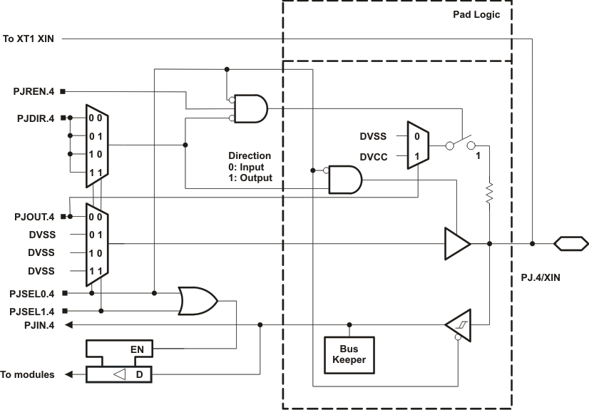
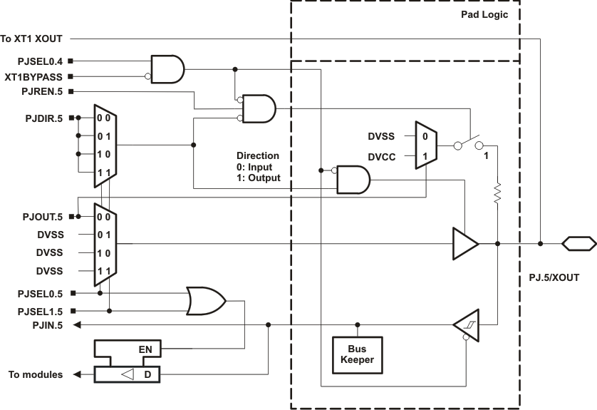
Table 6-14 Port PJ (PJ.4 and PJ.5) Pin Functions
| PIN NAME (P7.x) | x | FUNCTION | CONTROL BITS/SIGNALS (1) | |||||
|---|---|---|---|---|---|---|---|---|
| PJDIR.x | PJSEL1.5 | PJSEL0.5 | PJSEL1.4 | PJSEL0.4 | XT1 BYPASS | |||
| PJ.4/XIN | 4 | PJ.4 (I/O) | I: 0; O: 1 | X | X | 0 | 0 | X |
| XIN crystal mode (2) | X | X | X | 0 | 1 | 0 | ||
| XIN bypass mode (2) | X | X | X | 0 | 1 | 1 | ||
| PJ.5/XOUT | 5 | PJ.5 (I/O) | I: 0; O: 1 | 0 | 0 | 0 | 0 | X |
| XOUT crystal mode (2) | X | X | X | 0 | 1 | 0 | ||
| PJ.5 (I/O) (3) | I: 0; O: 1 | X | X | 0 | 1 | 1 | ||
(1) X = Don't care
(2) Setting PJSEL1.4 = 0 and PJSEL0.4 = 1 causes the general-purpose I/O to be disabled. When XT1BYPASS = 0, PJ.4 and PJ.5 are configured for crystal operation and PJSEL1.5 and PJSEL0.5 are do not care. When XT1BYPASS = 1, PJ.4 is configured for bypass operation and PJ.5 is configured as general-purpose I/O.
(3) When PJ.4 is configured in bypass mode, PJ.5 is configured as general-purpose I/O.