SLOS070D July 1979 – November 2014 NE5534 , NE5534A , SA5534 , SA5534A
PRODUCTION DATA.
- 1 Features
- 2 Applications
- 3 Description
- 4 Simplified Schematic
- 5 Revision History
- 6 Pin Configuration and Functions
- 7 Specifications
- 8 Detailed Description
- 9 Application and Implementation
- 10Power Supply Recommendations
- 11Layout
- 12Device and Documentation Support
- 13Mechanical, Packaging, and Orderable Information
Package Options
Refer to the PDF data sheet for device specific package drawings
Mechanical Data (Package|Pins)
- D|8
- P|8
Thermal pad, mechanical data (Package|Pins)
Orderable Information
9 Application and Implementation
NOTE
Information in the following applications sections is not part of the TI component specification, and TI does not warrant its accuracy or completeness. TI’s customers are responsible for determining suitability of components for their purposes. Customers should validate and test their design implementation to confirm system functionality.
9.1 General Application
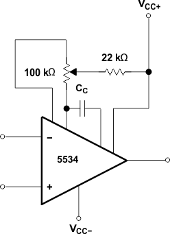
The input offset voltage of operational amplifiers (op amps) arises from unavoidable mismatches in the differential input stage of the op-amp circuit caused by mismatched transistor pairs, collector currents, current-gain betas (β), collector or emitter resistors, and so on. The input offset pins allow the designer to adjust for these mismatches by external circuitry. These input mismatches can be adjusted by putting resistors or a potentiometer between the inputs as shown in Figure 10. A potentiometer can be used to fine tune the circuit during testing or for applications which require precision offset control. More information about designing using the input-offset pins, see Offset Voltage of Operational Amplifiers (SLOA045).
9.2 Typical Application
The voltage follower configuration of the operational amplifier is used for applications where a weak signal is used to drive a relatively high current load. This circuit is also called a buffer amplifier or unity gain amplifier. The inputs of an operational amplifier have a very high resistance which puts a negligible current load on the voltage source. The output resistance of the operational amplifier is almost negligible, so it can provide as much current as necessary to the output load.
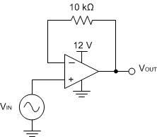 Figure 11. Voltage Follower Schematic
9.2.1 Design Requirements
- Output range of 2 V to 11 V
- Input range of 2 V to 11 V
9.2.2 Detailed Design Procedure
9.2.2.1 Output Voltage Swing
The output voltage of an operational amplifier is limited by its internal circuitry to some level below the supply rails. For this amplifier, the output voltage swing is within ±12 V, which accommodates the input and output voltage requirements.
9.2.2.2 Supply and Input Voltage
For correct operation of the amplifier, neither input must be higher than the recommended positive supply rail voltage or lower than the recommended negative supply rail voltage. The chosen amplifier must be able to operate at the supply voltage that accommodates the inputs. Because the input for this application goes up to
11 V, the supply voltage must be 12 V. Using a negative voltage on the lower rail rather than ground, allows the amplifier to maintain linearity for inputs below 2 V.
9.2.3 Application Curves for Output Characteristics
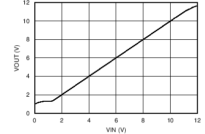 Figure 12. Output Voltage vs Input Voltage
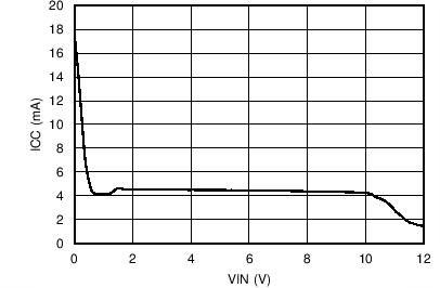 Figure 14. Current Drawn from Supply (ICC) vs the Input Voltage
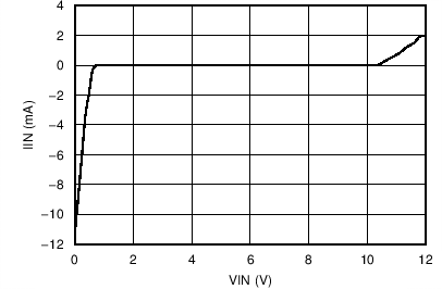 Figure 13. Current Drawn by the Input of the Voltage Follower (IIN) vs the Input Voltage