SLOS070D July 1979 – November 2014 NE5534 , NE5534A , SA5534 , SA5534A
PRODUCTION DATA.
- 1 Features
- 2 Applications
- 3 Description
- 4 Simplified Schematic
- 5 Revision History
- 6 Pin Configuration and Functions
- 7 Specifications
- 8 Detailed Description
- 9 Application and Implementation
- 10Power Supply Recommendations
- 11Layout
- 12Device and Documentation Support
- 13Mechanical, Packaging, and Orderable Information
Package Options
Refer to the PDF data sheet for device specific package drawings
Mechanical Data (Package|Pins)
- D|8
- P|8
Thermal pad, mechanical data (Package|Pins)
Orderable Information
7 Specifications
7.1 Absolute Maximum Ratings
over operating free-air temperature range (unless otherwise noted)(1)| MIN | TYP | MAX | UNIT | |||
|---|---|---|---|---|---|---|
| VCC | Supply voltage(2) | VCC+ | 0 | 22 | V | |
| VCC– | –22 | 0 | V | |||
| Input voltage, either input(2)(3) | VCC– | VCC+ | V | |||
| Input current(4) | –10 | 10 | mA | |||
| Duration of output short circuit(5) | Unlimited | |||||
| TJ | Operating virtual-junction temperature | 150 | °C | |||
(1) Stresses beyond those listed under Absolute Maximum Ratings may cause permanent damage to the device. These are stress ratings only, and functional operation of the device at these or any other conditions beyond those indicated under Recommended Operating Conditions is not implied. Exposure to absolute-maximum-rated conditions for extended periods may affect device reliability.
(2) All voltage values, except differential voltages, are with respect to the midpoint between VCC+ and VCC–.
(3) The magnitude of the input voltage must never exceed the magnitude of the supply voltage.
(4) Excessive current will flow if a differential input voltage in excess of approximately 0.6 V is applied between the inputs, unless some limiting resistance is used.
(5) The output may be shorted to ground or either power supply. Temperature and/or supply voltages must be limited to ensure the maximum dissipation rating is not exceeded.
(6) Maximum power dissipation is a function of TJ(max), θJA, and TA. The maximum allowable power dissipation at any allowable ambient temperature is PD = (TJ(max) – TA) / θJA. Operating at the absolute maximum TJ of 150°C can affect reliability.
(7) The package thermal impedance is calculated in accordance with JESD 51-7.
7.2 Handling Ratings
| MIN | MAX | UNIT | ||||
|---|---|---|---|---|---|---|
| Tstg | Storage temperature range | –65 | 150 | °C | ||
| V(ESD) | Electrostatic discharge | Human body model (HBM), per ANSI/ESDA/JEDEC JS-001, all pins | 0 | 2000 | V | |
| Charged device model (CDM), per JEDEC specification JESD22-C101, all pins | 0 | 200 | ||||
7.3 Recommended Operating Conditions
| MIN | MAX | UNIT | |||
|---|---|---|---|---|---|
| VCC | Supply voltage | VCC+ | 5 | 15 | V |
| VCC– | –5 | –15 | V | ||
| TA | Operating free-air temperature | NE5534, NE5534A | 0 | 70 | °C |
| SA5534, SA5534A | –40 | 85 | |||
7.4 Thermal Information
| THERMAL METRIC(1) | NE5534, NE5534A SA5534, and SA5534A |
UNIT | |||
|---|---|---|---|---|---|
| D | P | PS | |||
| 8 PINS | |||||
| RθJA | Package thermal impedance(7)(6) | 97 | 85 | 95 | °C/W |
(1) For more information about traditional and new thermal metrics, see the IC Package Thermal Metrics application report (SPRA953).
7.5 Electrical Characteristics
VCC± = ±15 V, TA = 25°C (unless otherwise noted)| PARAMETER | TEST CONDITIONS(1) | MIN | TYP | MAX | UNIT | ||
|---|---|---|---|---|---|---|---|
| VIO | Input offset voltage | VO = 0 RS = 50 Ω |
TA = 25°C | 0.5 | 4 | mV | |
| TA = Full range | 5 | ||||||
| IIO | Input offset current | VO = 0 | TA = 25°C | 20 | 300 | nA | |
| TA = Full range | 400 | ||||||
| IIB | Input bias current | VO = 0 | TA = 25°C | 500 | 1500 | nA | |
| TA = Full range | 2000 | ||||||
| VICR | Common-mode input-voltage range | ±12 | ±13 | V | |||
| VO(PP) | Maximum peak-to-peak output-voltage swing | RL ≥ 600 Ω | VCC± = ±15 V | 24 | 26 | V | |
| VCC± = ±18 V | 30 | 32 | |||||
| AVD | Large-signal differential-voltage amplification | VO = ±10 V RL ≥ 600 Ω, |
TA = 25°C | 25 | 100 | V/mV | |
| TA = Full range | 15 | ||||||
| RL ≥ 2 kΩ, VO±10 V | TA = 25°C | 25 | 100 | ||||
| TA = Full range | 15 | ||||||
| Avd | Small-signal differential-voltage amplification | f = 10 kHz | CC = 0 | 6 | V/mV | ||
| CC = 22 pF | 2.2 | ||||||
| BOM | Maximum output-swing bandwidth | VO = ±10 V | CC = 0 | 200 | kHz | ||
| CC = 22 pF | 95 | ||||||
| VCC± 18 V, RL = 600 Ω |
VO = ±14 V CC = 22 pF |
70 | |||||
| B1 | Unity-gain bandwidth | CC = 22 pF | CL = 100 pF | 10 | MHz | ||
| ri | Input resistance | 30 | 100 | kΩ | |||
| zo | Output impedance | AVD = 30 dB, CC = 22 pF |
RL = 600 Ω, f = 10 kHz |
0.3 | Ω | ||
| CMRR | Common-mode rejection ratio | VO = 0, RS = 50 Ω |
VIC = VICRmin | 70 | 100 | dB | |
| kSVR | Supply-voltage rejection ratio (ΔVCC or ΔVIO) | VCC± = ±9 V to ±15 V, VO = 0 |
RS = 50 Ω | 80 | 100 | dB | |
| IOS | Output short-circuit current | 38 | mA | ||||
| ICC | Total supply current | VO = 0, No load | TA = 25°C | 4 | 8 | mA | |
(1) All characteristics are measured under open-loop conditions with zero common-mode input voltage, unless otherwise specified. For NE5534 and NE5534A, full range is 0°C to 70°C. For SA5534 and SA5534A, full range is –40°C to 85°C.
7.6 Operating Characteristics
VCC± = ±15 V, TA = 25°C (unless otherwise noted)| PARAMETER | TEST CONDITIONS | NE5534, SA5534 | NE5534A, SA5534A | UNIT | ||||
|---|---|---|---|---|---|---|---|---|
| TYP | MIN | TYP | MAX | |||||
| SR | Slew rate | CC = 0 | 13 | 13 | V/μs | |||
| CC = 22 pF | 6 | 6 | ||||||
| tr | Rise time | VI = 50 mV, RL = 600 Ω, CL = 100 pF |
AVD = 1, CC = 22 pF |
20 | 20 | ns | ||
| Overshoot factor | 20 | 20 | % | |||||
| Rise time | VI = 50 mV, RL = 600 Ω, CL = 500 pF |
AVD = 1, CC = 47 pF |
50 | 50 | ns | |||
| Overshoot factor | 35% | 35% | — | |||||
| Vn | Equivalent input noise voltage | f = 30 Hz | 7 | 5.5 | 7 | nV/√Hz | ||
| f = 1 kHz | 4 | 3.5 | 4.5 | |||||
| In | Equivalent input noise current | f = 30 Hz | 2.5 | 1.5 | pA/√Hz | |||
| f = 1 kHz | 0.6 | 0.4 | ||||||
| F | Average noise figure | RS = 5 kΩ | f = 10Hz to 20 kHz | 0.9 | dB | |||
7.7 Typical Characteristics
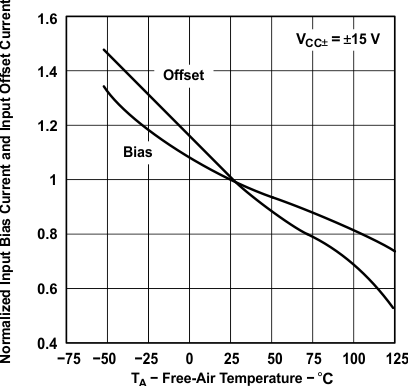 Figure 1. Normalized Input Bias Current and Input Offset Current
 vs Free-Air Temperature
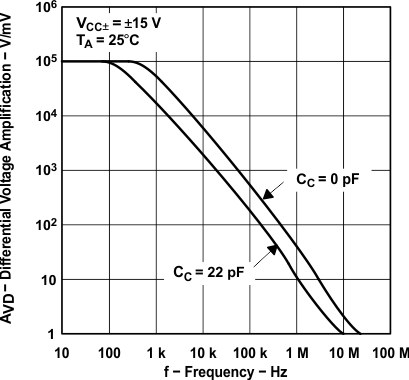 Figure 3. Large-Signal Differential Voltage Amplification
 vs Frequency
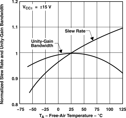 Figure 5. Normalized Slew Rate and Unity-Gain Bandwidth
 vs Free-Air Temperature
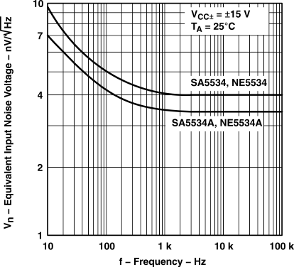 Figure 7. Equivalent Input Noise Voltage
 vs Frequency
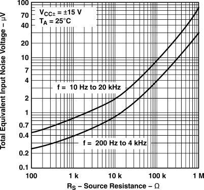 Figure 9. Total Equivalent Input Noise Voltage
 vs Source Resistance
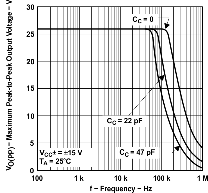 Figure 2. Maximum Peak-to-Peak Output Voltage
 vs Frequency
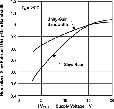 Figure 4. Normalized Slew Rate and Unity-Gain Bandwidth
 vs Supply Voltage
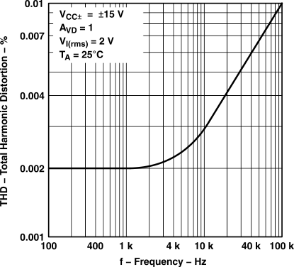 Figure 6. Total Harmonic Distortion
 vs Frequency
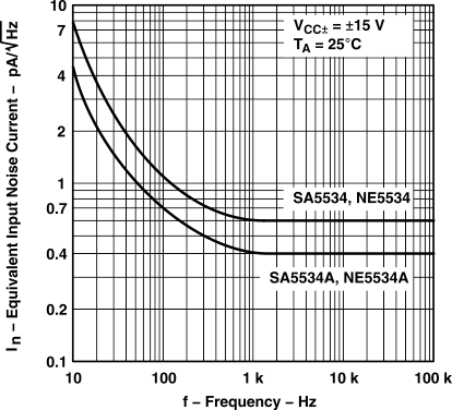 Figure 8. Equivalent Input Noise Current
 vs Frequency