SBOS727B November 2015 – May 2016 OPA1622
PRODUCTION DATA.
- 1 Features
- 2 Applications
- 3 Description
- 4 Revision History
- 5 Pin Configuration and Functions
- 6 Specifications
- 7 Detailed Description
- 8 Application and Implementation
- 9 Power Supply Recommendations
- 10Layout
- 11Device and Documentation Support
- 12Mechanical, Packaging, and Orderable Information
Package Options
Mechanical Data (Package|Pins)
- DRC|10
Thermal pad, mechanical data (Package|Pins)
- DRC|10
Orderable Information
7 Detailed Description
7.1 Overview
The OPA1622, dual, bipolar-input, audio operational amplifier uses a unique internal topology to deliver high output current with extremely low distortion while consuming minimal supply current. A single gain stage architecture, combining a high-gain transconductance input stage and a unity gain output stage, allows the OPA1622 to achieve an open-loop gain of 136 dB, even with 600-Ω loads.
The output stage of the OPA1622 is designed specifically to source and sink large amounts of current without degrading amplifier linearity. High-order distortion harmonics, produced by output stage crossover distortion, are greatly reduced with this design. The OPA1622 output stage also provides exceptionally low open-loop output impedance that improves stability with capacitive loads and is protected against short-circuit events.
A separate enable circuit maintains control of the input and output stage when the amplifier is placed into its shutdown mode and limits transients at the amplifier output when transitioning to and from this state. The enable circuit features logic levels referenced to the amplifier ground pin. This configuration simplifies the interface between the amplifier and the ground-referenced GPIO pins of microcontrollers. The addition of a ground pin to the amplifier provides several additional benefits. For example, the compensation capacitor between the input and output stages of the OPA1622 is referenced to the ground pin, greatly improving PSRR.
7.2 Functional Block Diagram
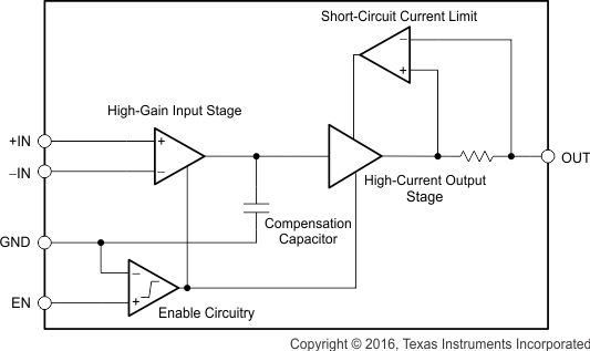 Figure 41. OPA1622 Simplified Schematic
7.3 Feature Description
7.3.1 Power Dissipation
The OPA1622 is capable of high output current with power-supply voltages up to ±18 V. Internal power dissipation increases when operating at high supply voltages. The power dissipated in the op amp (POPA) is calculated using Equation 1:

In order to calculate the worst-case power dissipation in the op amp, the ac and dc cases must be considered separately.
In the case of constant output current (dc) to a resistive load, the maximum power dissipation in the op amp occurs when the output voltage is half the positive supply voltage. This calculation assumes that the op amp is sourcing current from the positive supply to a grounded load. If the op amp sinks current from a grounded load, modify Equation 2 to include the negative supply voltage instead of the positive.

The maximum power dissipation in the op amp for a sinusoidal output current (ac) to a resistive load occurs when the peak output voltage is 2/π times the supply voltage, given symmetrical supply voltages:

The dominant pathway for the OPA1622 to dissipate heat is through the package thermal pad and pins to the PCB. Copper leadframe construction used in the OPA1622 improves heat dissipation compared to conventional materials. PCB layout greatly affects thermal performance. Connect the OPA1622 package thermal pad to a copper pour at the most negative supply potential. This copper pour can be connected to a larger copper plane within the PCB using vias to improve power dissipation. Figure 42 shows an analogous thermal circuit that can be used for approximating the junction temperature of the OPA1622. The power dissipated in the OPA1622 is represented by current source PD; the ambient temperature is represented by voltage source 25ºC; and the junction-to-board and board-to-ambient thermal resistances are represented by resistors θJB and θBA, respectively. The board-to-ambient thermal resistance is unique to every application. The sum of θJB and θBA is the junction-to-ambient thermal resistance of the system. The value for junction-to-ambient thermal resistance reported in the Thermal Information table is determined using the JEDEC standard test PCB. The voltages in the analogous thermal circuit at the points TJ and TPCB represent the OPA1622 junction and PCB temperatures, respectively.
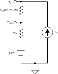 Figure 42. Approximate Thermal System Model of the OPA1622 Soldered to a PCB.
7.3.2 Thermal Shutdown
If the junction temperature of the OPA1622 exceeds 175ºC, a thermal shutdown circuit disables the amplifier in order to protect the device from damage. The amplifier is automatically re-enabled after the junction temperature falls below approximately 160ºC. If the condition that caused excessive power dissipation has not been removed, the amplifier oscillates between a shutdown and enabled state until the output fault is corrected.
7.3.3 Enable Pin
The enable pin (EN) of the OPA1622 is used to toggle the amplifier enabled and disabled states. The logic levels defining these two states are: VEN ≤ 0.78 V (shutdown mode), and VEN ≥ 0.82 V (enabled). These threshold levels are referenced to the device ground pin. The enable pin can be driven by a GPIO pin from the system controller, discrete logic gates, or can be connected directly to the V+ supply. Do not leave the enable pin floating because the amplifier is prevented from being enabled. Likewise, do not place GPIO pins used to control the enable pin in a high-impedance state because this placement also prevents the amplifier from being enabled. A small current flows into the enable pin when a voltage is applied. Using the simplified internal schematic shown in Figure 43, use Equation 4 to estimate the enable pin current:

As illustrated in Figure 43, the enable pin is protected by diodes to the amplifier power supplies. Do not connect the enable pin to voltages outside the limits defined in the Specifications section.
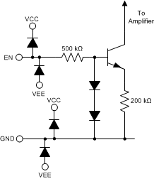 Figure 43. Enable Pin Simplified Internal Schematic
7.3.4 Ground Pin
The inclusion of a ground pin in the OPA1622 architecture allows the internal enable circuitry to be referenced to the system ground, eliminating the need for level shifting circuitry in many applications. The internal amplifier compensation capacitors are also referenced to this pin, greatly increasing the ac PSRR. For highest performance, connect the ground pin to a low-impedance reference point with minimal noise present. As shown in Figure 43, the ground pin is protected by ESD diodes to the amplifier power supplies. Do not connect the ground pin to voltages outside the limits defined in the Specifications section.
7.3.5 Electrical Overstress
Designers often ask questions about the capability of an operational amplifier to withstand electrical overstress. These questions tend to focus on the device inputs, but can involve the supply voltage pins or even the output pin. Each of these different pin functions have electrical stress limits determined by the voltage breakdown characteristics of the particular semiconductor fabrication process and specific circuits connected to the pin. Additionally, internal electrostatic discharge (ESD) protection is built into these circuits to protect them from accidental ESD events both before and during product assembly.
Having a good understanding of this basic ESD circuitry and its relevance to an electrical overstress event is helpful. Figure 44 shows the ESD circuits contained in the OPA1622. The ESD protection circuitry involves several current-steering diodes connected from the input and output pins and routed back to the internal power-supply lines, where they meet at an absorption device internal to the operational amplifier. This protection circuitry is intended to remain inactive during normal circuit operation.
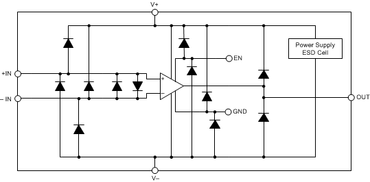 Figure 44. Equivalent Internal ESD Circuitry
7.3.6 Input Protection
The input pins of the OPA1622 are protected from excessive differential voltage with back-to-back diodes, as Figure 45 shows. In most circuit applications, the input protection circuitry has no consequence. However, in low-gain or G = +1 circuits, fast-ramping input signals can forward bias these diodes because the output of the amplifier cannot respond quickly enough to the input ramp. If the input signal is fast enough to create this forward-bias condition, the input signal current must be limited to 10 mA or less. If the input signal current is not inherently limited, use an input series resistor (RI) or a feedback resistor (RF) to limit the signal input current. This input series resistor degrades the low-noise performance of the OPA1622 and is examined in the Noise Performance section. Figure 45 shows an example configuration when both current-limiting input and feedback resistors are used.
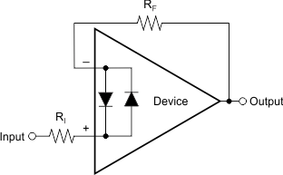 Figure 45. Pulsed Operation
7.4 Device Functional Modes
The OPA1622 has two operating modes determined by the voltage between the enable and ground pins: a shutdown mode (VEN ≤ 0.78V) and an enabled mode (VEN ≥ 0.82V). The measured datasheet performance parameters specified in the Typical Characteristics and Specifications sections are given with the amplifier in the enabled mode, unless otherwise noted.
7.4.1 Shutdown Mode
When the enable pin voltage is below the logic low threshold, the OPA1622 enters a shutdown mode with minimal power consumption. In this state the output transistors of the amplifier are not powered on. However, do not consider the amplifier output to be high-impedance. Applying signals to the output of the OPA1622 while the device is in the shutdown mode can parasitically power the output stage, causing the OPA1622 output to draw current.
The OPA1622 enable circuitry limits transients at the output when transitioning into or out of shutdown mode. However, small output transients do still accompany this transition, as illustrated in Figure 46 and Figure 47. Note that in both figures the time scale is 1 µs per division, indicating that the output transients are extremely brief in nature, and therefore not likely to be audible in headphone applications.
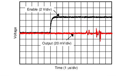 Figure 46. OPA1622 Output Voltage When Enable Pin Transitions High (32-Ω Load Connected)
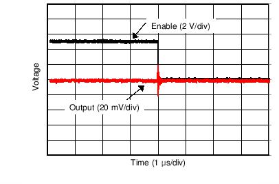 Figure 47. OPA1622 Output Voltage When Enable Pin Transitions Low (32-Ω Load Connected)
7.4.2 Output Transients During Power Up and Power Down
To minimize the possibility of output transients that might produce an audible click or pop, ramp the supply voltages for the OPA1622 symmetrically to their nominal values. Asymmetrical supply ramping can cause output transients during power up that can be audible in headphone applications. If possible, hold the enable pin low while the power supplies are ramping up or down. If the enable pin is not being independently controlled (for example, by a GPIO pin), use a voltage divider to hold the enable pin voltage below the logic-high threshold until the power supplies reach the specified minimum voltage, as shown in Figure 48.
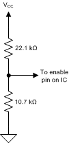 Figure 48. Voltage Divider Used to Hold Enable Low at Power-Up or Power-Down