SLOS805C July 2012 – August 2016 OPA1662-Q1
PRODUCTION DATA.
- 1 Features
- 2 Applications
- 3 Description
- 4 Revision History
- 5 Description Continued
- 6 Pin Configuration and Functions
- 7 Specifications
- 8 Detailed Description
- 9 Application and Implementation
- 10Power Supply Recommendations
- 11Layout
- 12Device and Documentation Support
- 13Mechanical, Packaging, and Orderable Information
Package Options
Mechanical Data (Package|Pins)
Thermal pad, mechanical data (Package|Pins)
Orderable Information
8 Detailed Description
8.1 Overview
The OPA1662-Q1 operational amplifier achieves a low 3.3 nV/√Hz noise density with an ultra-low distortion of 0.00006% at 1 kHz that makes the device suitable for audio application. This device has a wide supply range with excellent PSRR, making it a suitable option for applications that are battery powered without regulation.
8.2 Functional Block Diagram
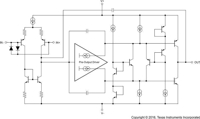 Figure 43. OPA1662-Q1 Simplified Schematic
8.3 Feature Description
8.3.1 Operating Voltage
The OPA1662-Q1 op amp operates from ±1.5-V to ±18-V supplies while maintaining excellent performance. The OPA1662-Q1 can operate with as little as 3 V between the supplies and up to 36 V between the supplies. However, some applications do not require equal positive and negative output voltage swing. With the OPA1662‑Q1 device, power-supply voltages do not need to be equal. For example, the positive supply could be set to 25 V with the negative supply at –5 V.
In all cases, the common-mode voltage must be maintained within the specified range. In addition, key parameters are assured over the specified temperature of TA = –40°C to 85°C. Parameters that vary significantly with operating voltage or temperature are shown in the Typical Characteristics.
8.3.2 Input Protection
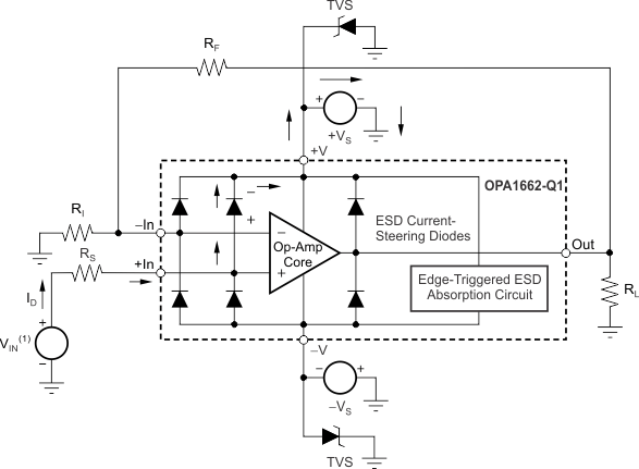
The input terminals of the OPA1662-Q1 are protected from excessive differential voltage with back-to-back diodes, as Figure 44 illustrates. In most circuit applications, the input protection circuitry has no consequence. However, in low-gain or G = 1 circuits, fast ramping input signals can forward bias these diodes because the output of the amplifier cannot respond rapidly enough to the input ramp. If the input signal is fast enough to create this forward bias condition, the input signal current must be limited to 10 mA or less. If the input signal current is not inherently limited, an input series resistor (RI) or a feedback resistor (RF) can be used to limit the signal input current. This resistor degrades the low-noise performance of the OPA1662-Q1 and is examined in Noise Performance. Figure 44 shows an example configuration when both current-limiting input and feedback resistors are used.
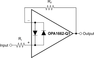 Figure 44. Pulsed Operation
8.3.3 Noise Performance
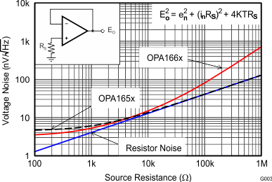
Figure 45 shows the total circuit noise for varying source impedances with the op amp in a unity-gain configuration (no feedback resistor network, and therefore no additional noise contributions).
The OPA1662-Q1 (GBW = 22 MHz, G = 1) is shown with total circuit noise calculated. The op amp itself contributes both a voltage noise component and a current noise component. The voltage noise is commonly modeled as a time-varying component of the offset voltage. The current noise is similarly modeled as the time-varying component of the input bias current and reacts with the source resistance to create a voltage component of noise. Therefore, the lowest noise op amp for a given application depends on the source impedance. For low source impedance, current noise is negligible, and voltage noise generally dominates. The low voltage noise of the OPA1662-Q1 op amp makes them a better choice for low source impedances of less than 1 kΩ.
- en is the voltage noise
- in is the current noise
- RS is the source impedance
- k is Boltzmann’s constant = 1.38 × 10⁻²³ J/K
- T is the temperature in Kelvins (K)
8.3.4 Basic Noise Calculations
Design of low-noise op amp circuits requires careful consideration of a variety of possible noise contributors: noise from the signal source, noise generated in the op amp, and noise from the feedback network resistors. The total noise of the circuit is the root-sum-square combination of all noise components.
The resistive portion of the source impedance produces thermal noise proportional to the square root of the resistance. Figure 45 plots this equation. The source impedance is usually fixed; consequently, select the op amp and the feedback resistors to minimize the respective contributions to the total noise.
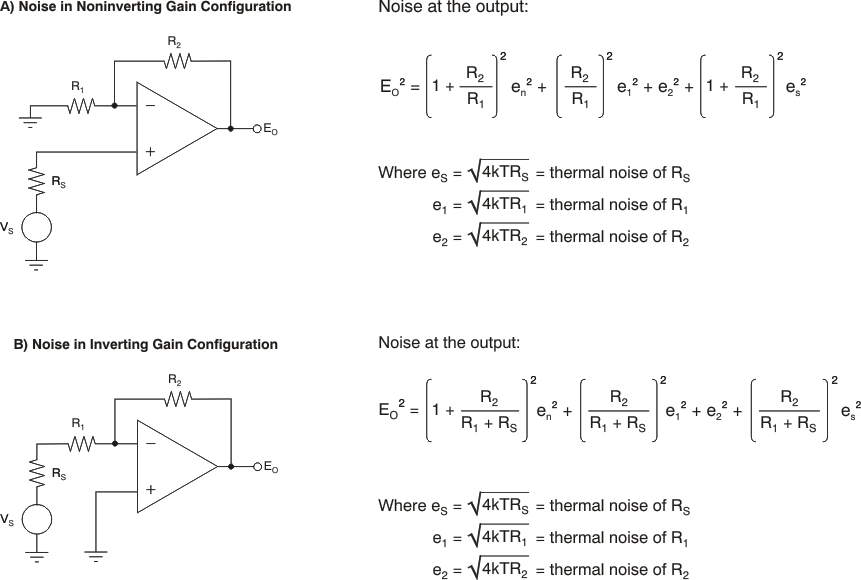
Figure 46 illustrates both inverting and noninverting op amp circuit configurations with gain. In circuit configurations with gain, the feedback network resistors also contribute noise. The current noise of the op amp reacts with the feedback resistors to create additional noise components. The feedback resistor values can generally be chosen to make these noise sources negligible. The equations for total noise are shown for both configurations.
8.3.5 Total Harmonic Distortion Measurements
The OPA1662-Q1 op amp has excellent distortion characteristics. THD + noise is below 0.0006% (G = 1, VO = 3 VRMS, BW = 80 kHz) throughout the audio frequency range, 20 Hz to 20 kHz, with a 2-kΩ load (see Figure 7 for characteristic performance).
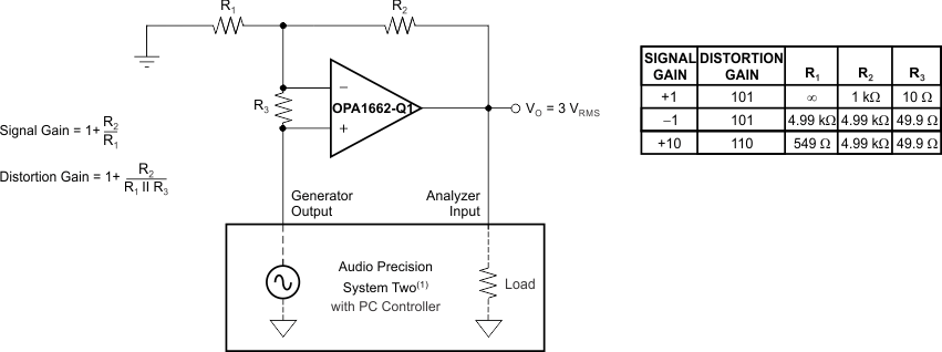
The distortion produced by the OPA1662-Q1 op amp is below the measurement limit of many commercially available distortion analyzers. However, a special test circuit (such as Figure 47 shows) can be used to extend the measurement capabilities.
Op amp distortion can be considered an internal error source that can be referred to the input. Figure 47 shows a circuit that causes the op amp distortion to be gained up (see the table in Figure 47 for the distortion gain factor for various signal gains). The addition of R3 to the otherwise standard noninverting amplifier configuration alters the feedback factor or noise gain of the circuit. The closed-loop gain is unchanged, but the feedback available for error correction is reduced by the distortion gain factor, thus extending the resolution by the same amount. The input signal and load applied to the op amp are the same as with conventional feedback without R3. The value of R3 must be kept small to minimize its effect on the distortion measurements.
The validity of this technique can be verified by duplicating measurements at high gain or high frequency where the distortion is within the measurement capability of the test equipment. Measurements for this data sheet were made with an Audio Precision System Two distortion and noise analyzer, which greatly simplifies such repetitive measurements. The measurement technique can, however, be performed with manual distortion measurement instruments.
8.3.6 Capacitive Loads
The dynamic characteristics of the OPA1662-Q1 have been optimized for commonly encountered gains, loads, and operating conditions. The combination of low closed-loop gain and high capacitive loads decreases the phase margin of the amplifier and can lead to gain peaking or oscillations. As a result, heavier capacitive loads must be isolated from the output. The simplest way to achieve this isolation is to add a small resistor (RS equal to 50 Ω, for example) in series with the output.
This small series resistor also prevents excess power dissipation if the output of the device becomes shorted. Figure 25 illustrates a graph of Small-Signal Overshoot vs Capacitive Load for several values of RS. Also see Applications Bulletin: Feedback Plots Define Op Amp AC Performance for details of analysis techniques and application circuits.
8.3.7 Electrical Overstress
Designers often ask questions about the capability of an operational amplifier to withstand electrical overstress. These questions tend to focus on the device inputs, but may involve the supply voltage pins or even the output pin. Each of these different pin functions have electrical stress limits determined by the voltage breakdown characteristics of the particular semiconductor fabrication process and specific circuits connected to the pin. Additionally, internal electrostatic discharge (ESD) protection is built into these circuits to protect them from accidental ESD events both before and during product assembly.
It is helpful to have a good understanding of this basic ESD circuitry and its relevance to an electrical overstress event. Figure 48 illustrates the ESD circuits contained in the OPA1662-Q1 (indicated by the dashed line area). The ESD protection circuitry involves several current-steering diodes connected from the input and output pins and routed back to the internal power-supply lines, where they meet at an absorption device internal to the operational amplifier. This protection circuitry is intended to remain inactive during normal circuit operation.
An ESD event produces a short duration, high-voltage pulse that is transformed into a short duration, high-current pulse as it discharges through a semiconductor device. The ESD protection circuits are designed to provide a current path around the operational amplifier core to prevent it from being damaged. The energy absorbed by the protection circuitry is then dissipated as heat.
When an ESD voltage develops across two or more of the amplifier device pins, current flows through one or more of the steering diodes. Depending on the path that the current takes, the absorption device may activate. The absorption device internal to the OPA1662-Q1 triggers when a fast ESD voltage pulse is impressed across the supply pins. Once triggered, it quickly activates, clamping the ESD pulse to a safe voltage level.
When the operational amplifier connects into a circuit such as that illustrated in Figure 48, the ESD protection components are intended to remain inactive and not become involved in the application circuit operation. However, circumstances may arise where an applied voltage exceeds the operating voltage range of a given pin. If this condition occurs, there is a risk that some of the internal ESD protection circuits may be biased on, and conduct current. Any such current flow occurs through steering diode paths and rarely involves the absorption device.
Figure 48 depicts a specific example where the input voltage, VIN, exceeds the positive supply voltage (+VS) by 500 mV or more. Much of what happens in the circuit depends on the supply characteristics. If +VS can sink the current, one of the upper input steering diodes conducts and directs current to +VS. Excessively high current levels can flow with increasingly higher VIN. As a result, TI recommends that applications limit the input current to 10 mA.
If the supply is not capable of sinking the current, VIN may begin sourcing current to the operational amplifier, and then take over as the source of positive supply voltage. The danger in this case is that the voltage can rise to levels that exceed the operational amplifier absolute maximum ratings. In extreme but rare cases, the absorption device triggers on while +VS and –VS are applied. If this event happens, a direct current path is established between the +VS and –VS supplies. The power dissipation of the absorption device is quickly exceeded, and the extreme internal heating destroys the operational amplifier.
Another common question involves what happens to the amplifier if an input signal is applied to the input while the power supplies +VS or –VS are at 0 V. Again, it depends on the supply characteristic while at 0 V, or at a level below the input signal amplitude. If the supplies appear as high impedance, then the operational amplifier supply current may be supplied by the input source through the current steering diodes. This state is not a normal bias condition; the amplifier most likely will not operate normally. If the supplies are low impedance, then the current through the steering diodes can become quite high. The current level depends on the ability of the input source to deliver current, and any resistance in the input path.
If there is an uncertainty about the ability of the supply to absorb this current, external Zener diodes may be added to the supply pins as shown in Figure 48.
The Zener voltage must be selected such that the diode does not turn on during normal operation. However, its Zener voltage must be low enough so that the Zener diode conducts if the supply pin begins to rise above the safe operating supply voltage level.
8.4 Device Functional Modes
The OPA1662-Q1 has a single functional mode and is operational when the power-supply voltage is greater than 3 V (±1.5 V). The maximum power supply voltage for the OPA1662-Q1 is 36 V (±18 V).
