SBOS008A September 2000 – September 2023 OPA177
PRODUCTION DATA
- 1
- 1Features
- 2Applications
- 3Description
- 4Revision History
- 5Pin Configuration and Functions
- 6Specifications
- 7Application and Implementation
- 8Device and Documentation Support
- 9Mechanical, Packaging, and Orderable Information
Package Options
Refer to the PDF data sheet for device specific package drawings
Mechanical Data (Package|Pins)
- D|8
- P|8
Thermal pad, mechanical data (Package|Pins)
Orderable Information
5 Pin Configuration and Functions
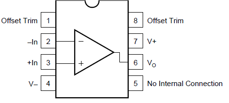
 Figure 5-1 D Package, 8-Pin SOIC
 and P Package, 8-Pin PDIP
(Top View)
Table 5-1 Pin Functions
| PIN | TYPE | DESCRIPTION | |
|---|---|---|---|
| NAME | NO. | ||
| +In | 3 | Input | Noninverting input |
| −In | 2 | Input | Inverting input |
| No Internal Connection | 5 | — | No internal connection (can be left floating) |
| Offset Trim | 1, 8 | — | Input offset voltage trim (leave floating if not used) |
| V+ | 7 | Power | Positive (highest) power supply |
| V− | 4 | Power | Negative (lowest) power supply |
| VO | 6 | Output | Output |