SBOS826D December   2017  – October 2019 OPA207

PRODUCTION DATA.  

  1. Features
  2. Applications
  3. Description
    1.     Device Images
      1.      Ultra-Low 0.1-Hz to 10-Hz Noise
  4. Revision History
  5. Pin Configuration and Functions
    1.     Pin Functions
  6. Specifications
    1. 6.1 Absolute Maximum Ratings
    2. 6.2 ESD Ratings
    3. 6.3 Recommended Operating Conditions
    4. 6.4 Thermal Information
    5. 6.5 Electrical Characteristics
    6. 6.6 Typical Characteristics
  7. Detailed Description
    1. 7.1 Overview
    2. 7.2 Functional Block Diagram
    3. 7.3 Feature Description
      1. 7.3.1 Operating Voltage
      2. 7.3.2 Input Protection
      3. 7.3.3 ESD Protection
      4. 7.3.4 Input Stage Linearization
      5. 7.3.5 Rail-to-Rail Output
      6. 7.3.6 Low Input Bias Current
      7. 7.3.7 Slew Boost
      8. 7.3.8 EMI Rejection Ratio (EMIRR)
    4. 7.4 Device Functional Modes
  8. Application and Implementation
    1. 8.1 Application Information
    2. 8.2 Typical Applications
      1. 8.2.1 Typical OPA207 Application
        1. 8.2.1.1 Design Requirements
        2. 8.2.1.2 Detailed Design Procedure
        3. 8.2.1.3 Application Curve
      2. 8.2.2 Precision Low-Side Current Sensing
      3. 8.2.3 Precision Buffer With Increased Output Current
  9. Power Supply Recommendations
  10. 10Layout
    1. 10.1 Layout Guidelines
    2. 10.2 Layout Example
  11. 11Device and Documentation Support
    1. 11.1 Device Support
      1. 11.1.1 Development Support
        1. 11.1.1.1 Webench Filter Designer Tool
        2. 11.1.1.2 TINA-TI (Free Software Download)
        3. 11.1.1.3 TI Precision Designs
    2. 11.2 Documentation Support
      1. 11.2.1 Related Documentation
    3. 11.3 Receiving Notification of Documentation Updates
    4. 11.4 Support Resources
    5. 11.5 Trademarks
    6. 11.6 Electrostatic Discharge Caution
  12. 12Mechanical, Packaging, and Orderable Information

Package Options

Mechanical Data (Package|Pins)
Thermal pad, mechanical data (Package|Pins)
Orderable Information

Precision Buffer With Increased Output Current

The OPA207 can be configured as illustrated in Figure 50 to drive low impedance loads. In Figure 50, the OPA207 is configured in a gain of +10 V/V, and the output current is boosted by the NPN (2N2904) and PNP (2N2906) bipolar transistors. For low output voltages the OPA207 supplies the load current directly through the 100-Ω resistor. The bipolar transistors begin to supply current when the voltage drop across the 100-Ω resistor exceeds approximately 500 mV. Figure 50 illustrates the results for a 50-Ω load resistor driven with a 10-V step at the output. This results in a 200-mA current supplied by the circuit.
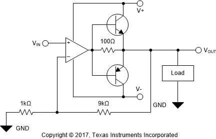
OPA207 OPA207_Precision_Buffer.gifFigure 50. Precision Buffer (G = 10 V/V) With High Output Drive Capability
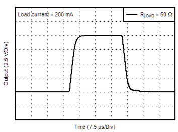
OPA207 Precision_Buffer.gifFigure 51. 50-Ω Load Driven With a 10-V Step