SBOS826D December 2017 – October 2019 OPA207
PRODUCTION DATA.
- 1 Features
- 2 Applications
- 3 Description
- 4 Revision History
- 5 Pin Configuration and Functions
- 6 Specifications
- 7 Detailed Description
- 8 Application and Implementation
- 9 Power Supply Recommendations
- 10Layout
- 11Device and Documentation Support
- 12Mechanical, Packaging, and Orderable Information
Package Options
Mechanical Data (Package|Pins)
Thermal pad, mechanical data (Package|Pins)
- DGK|8
Orderable Information
7.3.5 Rail-to-Rail Output
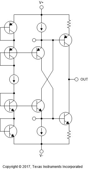
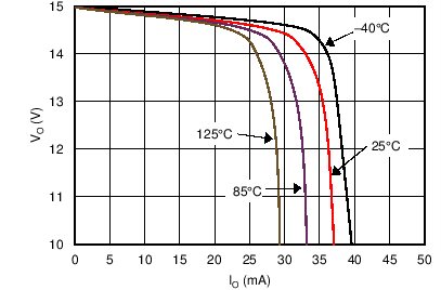
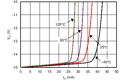
The OPA207 uses a rail-to-rail output stage capable of swinging within a few millivolts from either power supply rail while maintaining high open-loop gain. Figure 40 shows a simplified drawing of the output stage circuit. Resistors connected in series with each output transistor ensure a consistent output current limit. Limiting the output current in this way ensures reliable operation of the OPA207 under short circuited conditions and protects sensitive loads from being damaged by excessive current. Figure 41 and Figure 42 illustrate the maximum output current available from the OPA207 at various temperatures.
 Figure 40. Simplified Rail-to-Rail Output Stage Circuit
  Figure 41. Output Swing to Rail While Sourcing Current
  Figure 42. Output Swing to Rail While Sinking Current