SBOS110C May 1998 – March 2023 OPA2227 , OPA2228 , OPA227 , OPA228 , OPA4227 , OPA4228
PRODUCTION DATA
- 1 Features
- 2 Applications
- 3 Description
- 4 Revision History
- 5 Pin Configuration and Functions
-
6 Specifications
- 6.1 Absolute Maximum Ratings
- 6.2 ESD Ratings
- 6.3 Recommended Operating Conditions
- 6.4 Thermal Information: OPA227, OPA228
- 6.5 Thermal Information: OPA2227, OPA2228
- 6.6 Thermal Information: OPA4227, OPA4228
- 6.7 Electrical Characteristics: OPAx227
- 6.8 Electrical Characteristics: OPAx228
- 6.9 Typical Characteristics
- 7 Detailed Description
-
8 Application and Implementation
- 8.1 Application Information
- 8.2 Typical Application
- 8.3 Power Supply Recommendations
- 8.4 Layout
- 9 Device and Documentation Support
- 10Mechanical, Packaging, and Orderable Information
Package Options
Mechanical Data (Package|Pins)
Thermal pad, mechanical data (Package|Pins)
- D|8
Orderable Information
8.2.1.2 Detailed Design Procedure
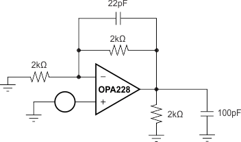
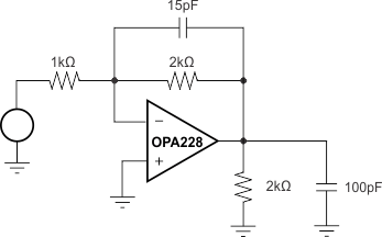
A variety of compensation techniques have been evaluated specifically for use with the OPA228. The recommended configuration consists of an additional capacitor (CF) in parallel with the feedback resistance, as shown in Figure 8-2 and Figure 8-3. This feedback capacitor serves two purposes in compensating the circuit. The operational amplifier’s input capacitance and the feedback resistors interact to cause phase shift that can result in instability. CF compensates the input capacitance, minimizing peaking. Additionally, at high frequencies, the closed-loop gain of the amplifier is strongly influenced by the ratio of the input capacitance and the feedback capacitor. Thus, CF can be selected to yield good stability while maintaining high-speed.
Without external compensation, the noise specification of the OPA228 is the same as that for the OPA227 in gains of 5 or greater. With the additional external compensation, the output noise of the OPA228 is higher. The amount of noise increase is directly related to the increase in high-frequency closed-loop gain established by the CIN/CF ratio.
Figure 8-2 and Figure 8-3 show the recommended circuit for gains of 2 and –2, respectively. The figures suggest approximate values for CF. Because compensation highly depends on circuit design, board layout, and load conditions, optimize CF experimentally for best results. Figure 8-4 and Figure 8-6 show the large- and small-signal step responses for the G = 2 configuration with 100-pF load capacitance.Figure 8-5 and Figure 8-7 show the large- and small-signal step responses for the G = –2 configuration with 100-pF load capacitance.
 Figure 8-2 Compensation of the OPA228 for G = 2
 Figure 8-3 Compensation for OPA228 for G = –2