SBOS110C May   1998  – March 2023 OPA2227 , OPA2228 , OPA227 , OPA228 , OPA4227 , OPA4228

PRODUCTION DATA  

  1. Features
  2. Applications
  3. Description
  4. Revision History
  5. Pin Configuration and Functions
  6. Specifications
    1. 6.1 Absolute Maximum Ratings
    2. 6.2 ESD Ratings
    3. 6.3 Recommended Operating Conditions
    4. 6.4 Thermal Information: OPA227, OPA228
    5. 6.5 Thermal Information: OPA2227, OPA2228
    6. 6.6 Thermal Information: OPA4227, OPA4228
    7. 6.7 Electrical Characteristics: OPAx227 
    8. 6.8 Electrical Characteristics: OPAx228 
    9. 6.9 Typical Characteristics
  7. Detailed Description
    1. 7.1 Overview
    2. 7.2 Functional Block Diagram
    3. 7.3 Feature Description
      1. 7.3.1 Offset Voltage and Drift
      2. 7.3.2 Operating Voltage
      3. 7.3.3 Offset Voltage Adjustment
      4. 7.3.4 Input Protection
      5. 7.3.5 Input Bias Current Cancellation
      6. 7.3.6 Noise Performance
      7. 7.3.7 Basic Noise Calculations
      8. 7.3.8 EMI Rejection Ratio (EMIRR)
        1. 7.3.8.1 EMIRR IN+ Test Configuration
    4. 7.4 Device Functional Modes
  8. Application and Implementation
    1. 8.1 Application Information
    2. 8.2 Typical Application
      1. 8.2.1 Using the OPAx228 in Low Gains
        1. 8.2.1.1 Design Requirements
        2. 8.2.1.2 Detailed Design Procedure
        3. 8.2.1.3 Application Curves
      2. 8.2.2 Three-Pole, 20 kHz Low Pass, 0.5-dB Chebyshev Filter
      3. 8.2.3 Long-Wavelength Infrared Detector Amplifier
      4. 8.2.4 High Performance Synchronous Demodulator
      5. 8.2.5 Headphone Amplifier
      6. 8.2.6 Three-Band Active Tone Control (Bass, Midrange, and Treble)
    3. 8.3 Power Supply Recommendations
    4. 8.4 Layout
      1. 8.4.1 Layout Guidelines
      2. 8.4.2 Layout Example
  9. Device and Documentation Support
    1. 9.1 Device Support
      1. 9.1.1 Development Support
        1. 9.1.1.1 TINA-TI™ Simulation Software (Free Download)
        2. 9.1.1.2 TI Reference Designs
    2. 9.2 Documentation Support
      1. 9.2.1 Related Documentation
    3. 9.3 Receiving Notification of Documentation Updates
    4. 9.4 Support Resources
    5. 9.5 Trademarks
    6. 9.6 Electrostatic Discharge Caution
    7. 9.7 Glossary
  10. 10Mechanical, Packaging, and Orderable Information

Package Options

Mechanical Data (Package|Pins)
Thermal pad, mechanical data (Package|Pins)
Orderable Information

Typical Characteristics

At TA = 25°C, RL = 10 kΩ, and VS = ±15 V, unless otherwise noted.
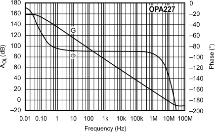
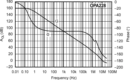
GUID-AF17A4C9-855E-4EDF-A42A-D7D6FB5663F0-low.gif
 
Figure 6-1 Open-Loop Gain and Phase vs Frequency
GUID-8FBD8644-A715-47A1-A751-9BFA7A6D2C0F-low.gif
 
 
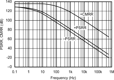
Figure 6-3 Power Supply and Common-Mode Rejection Ratio vs Frequency
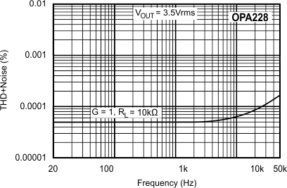
GUID-61953AF6-80C1-42F4-825D-27CAE76F4EE6-low.gif
 
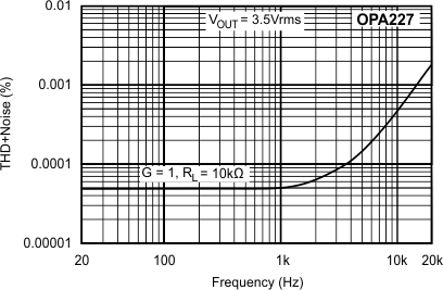
Figure 6-5 Total Harmonic Distortion + Noise vs Frequency
GUID-B3FF98B5-A819-40FE-968B-DFBFEB85CD50-low.gif
 
 
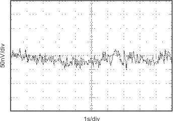
Figure 6-7 Input Noise Voltage vs Time
GUID-1728B7C1-664E-4EF8-A140-80719D189890-low.gif
 
 
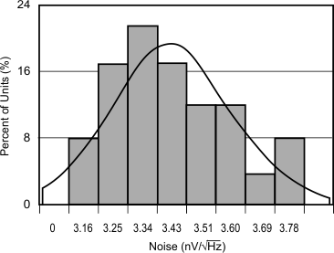
Figure 6-9 Voltage Noise Distribution (10 Hz)
GUID-00EEB7A4-A8BD-4C22-8E51-1053FA4929DB-low.gif
 
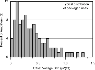
Figure 6-11 Offset Voltage Drift Production Distribution
GUID-B686304A-9FC1-4A5D-904B-07B421B7C2C5-low.gif
 
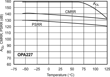
Figure 6-13 AOL, CMRR, PSRR vs Temperature
GUID-62A0E5E7-7BA2-466C-A956-9E9F6E7C0E9E-low.gif
 
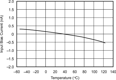
Figure 6-15 Input Bias Current vs Temperature
GUID-DE27934C-6495-42B1-B845-9B900801F314-low.gif
 
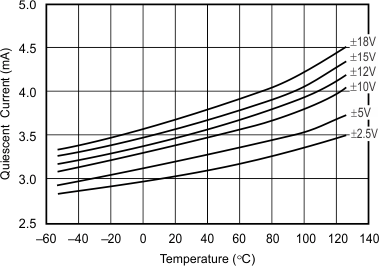
Figure 6-17 Quiescent Current vs Temperature
GUID-048E29E2-B26A-442D-A3F0-82D32A91E278-low.gif
 
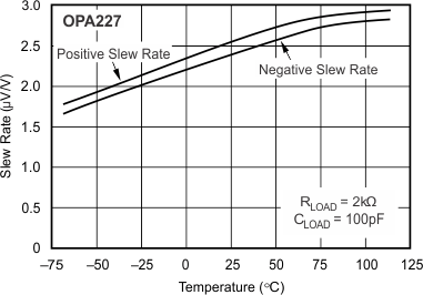
Figure 6-19 Slew Rate vs Temperature
GUID-49E15B08-95A7-4318-9515-7FFA5BF17A5E-low.gif
 
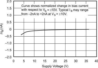
Figure 6-21 Change in Input Bias Current vs Power Supply Voltage
GUID-54CF0211-618B-4F1B-A891-8443C57C401F-low.gif
 
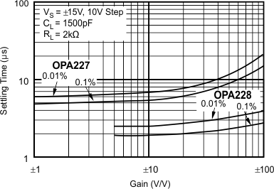
Figure 6-23 Settling Time vs Closed-Loop Gain
GUID-5E91DB11-0B97-49EF-9CC5-95A9884F2530-low.gif
 
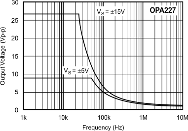
Figure 6-25 Maximum Output Voltage vs Frequency
GUID-AE403FCA-E885-4584-B01A-F857B7F81E33-low.gif
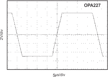
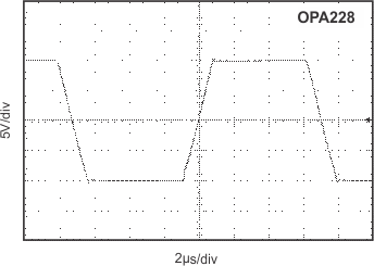
G = –1,CL = 1500 pF
Figure 6-27 Large-Signal Step Response
GUID-DDB34E6A-C26E-4D23-857D-06B708676033-low.gif
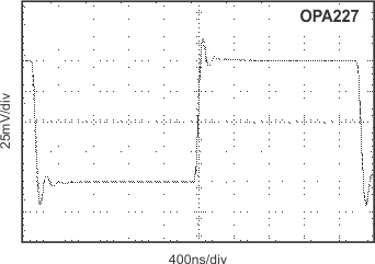
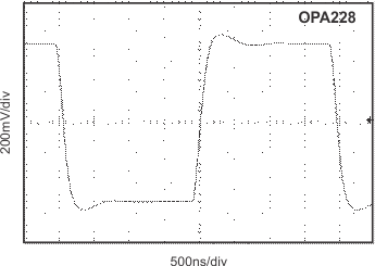
G = 1,CL = 5 pF
 
Figure 6-29 Small-Signal Step Response
GUID-A3071D87-DB93-49ED-B006-94216C95A08B-low.gif
 
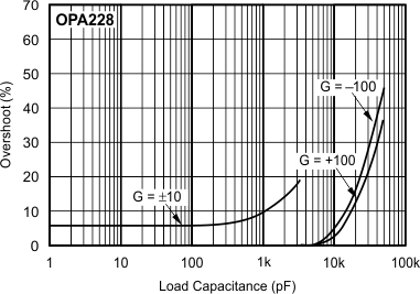
Figure 6-31 Small-Signal Overshoot vs Load Capacitance
GUID-DBEB9AB2-C831-45E9-A1CC-9067C1142DAD-low.gif
G = 10,CL = 1000 pFRL = 1.8 kΩ
Figure 6-33 Small-Signal Step Response
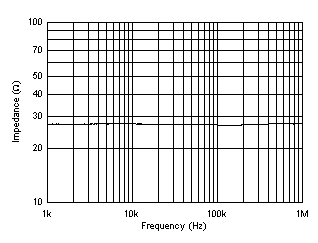
GUID-547DA468-0605-4D73-A8D2-1578E3D89E37-low.gif
 
Figure 6-35 Open-loop Output Impedance
GUID-FABFB9C6-4C98-4077-87EC-B4864AA60DBD-low.gif
 
Figure 6-2 Open-Loop Gain and Phase vs Frequency
GUID-41008E9F-5588-4AB3-9C56-1B1CA88B397F-low.gif
 
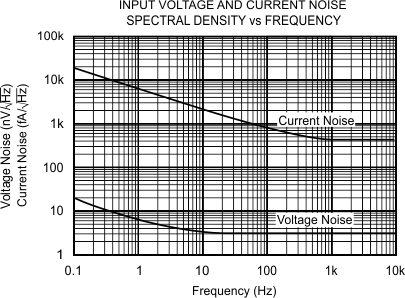
Figure 6-4 Input Voltage and Current Noise Spectral Density vs Frequency
GUID-1DC48ECF-D5FD-4DED-A1E3-9095559BFDE7-low.gif
 
Figure 6-6 Total Harmonic Distortion + Noise vs Frequency
GUID-EEFA8A41-4156-4DE9-B3DD-B6ACE64EC580-low.gif
 
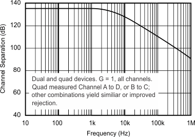
Figure 6-8 Channel Separation vs Frequency
GUID-DCDEACC6-0938-4C27-9B65-A4279336D4BE-low.gif
 
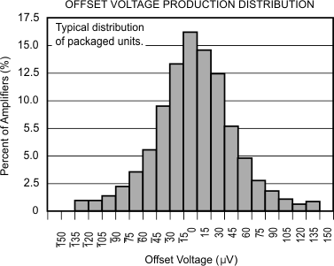
Figure 6-10 Offset Voltage Production Distribution
GUID-308CA2C5-758E-4421-B380-B0479AB34B36-low.gif
 
 
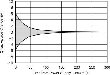
Figure 6-12 Warm-Up Offset Voltage Drift
GUID-5FAB1266-C67F-4743-8232-64E1190FCB83-low.gif
 
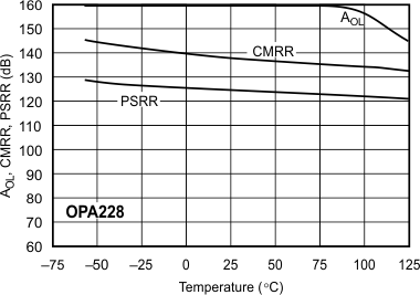
Figure 6-14 AOL, CMRR, PSRR vs Temperature
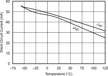
GUID-AC97231F-91B6-4210-A1A2-9A1455C167AF-low.gif
 
Figure 6-16 Short-Circuit Current vs Temperature
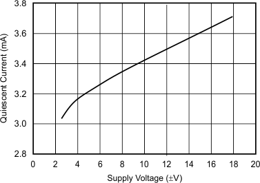
GUID-E3007809-832F-4266-A5B8-A546ACDAB92B-low.gif
 
Figure 6-18 Quiescent Current vs Supply Voltage
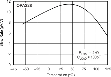
GUID-A1A5C6CF-C42A-4A25-8FD4-381A4E8E67E4-low.gif
 
Figure 6-20 Slew Rate vs Temperature
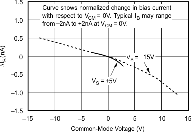
GUID-A8B102B6-CEE6-4DF9-AD57-22804E4B3C55-low.gif
 
Figure 6-22 Change in Input Bias Current vs Common-Mode Voltage
GUID-0DF8B591-79EA-4924-AE94-A24B05A9833E-low.gif
 
 
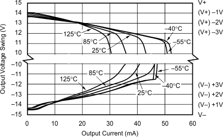
Figure 6-24 Output Voltage Swing vs Output Current
GUID-ADA30C23-BB25-424F-A6CB-1B58E374C950-low.gif
 
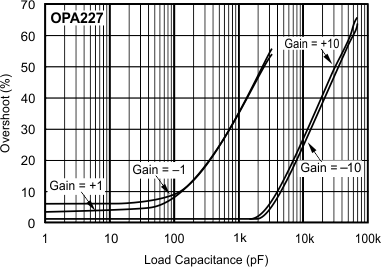
Figure 6-26 Small-Signal Overshoot vs Load Capacitance
GUID-8A83774B-1914-4B23-B622-D8D00E037F27-low.gif
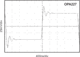
G = 1,C = 1000 pF
Figure 6-28 Small-Signal Step Response
GUID-BE964985-4F74-4940-BA28-90E895DE41C6-low.gif
 
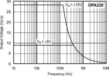
Figure 6-30 Maximum Output Voltage vs Frequency
GUID-D01D5A56-6ED9-4A2C-B7B8-902ED39CBF2B-low.gif
G = –10, CL = 100 pF
 
Figure 6-32 Large-Signal Step Response
GUID-79C81FD2-3778-4104-8ECB-5B7645FE6D9F-low.gif
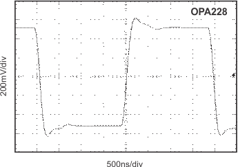
G = 10,CL = 1000 pFRL = 1.8 kΩ
Figure 6-34 Small-Signal Step Response