SBOS957D February   2022  – December 2023 OPA2328 , OPA328

PRODMIX  

  1.   1
  2. Features
  3. Applications
  4. Description
  5. Pin Configuration and Functions
  6. Specifications
    1. 5.1 Absolute Maximum Ratings
    2. 5.2 ESD Ratings
    3. 5.3 Recommended Operating Conditions
    4. 5.4 Thermal Information - OPA328
    5. 5.5 Thermal Information - OPA2328
    6. 5.6 Electrical Characteristics
    7. 5.7 Typical Characteristics
  7. Detailed Description
    1. 6.1 Overview
    2. 6.2 Functional Block Diagram
    3. 6.3 Feature Description
      1. 6.3.1 Input and ESD Protection
      2. 6.3.2 Rail-to-Rail Input
      3. 6.3.3 Phase Reversal
    4. 6.4 Device Functional Modes
  8. Application and Implementation
    1. 7.1 Application Information
      1. 7.1.1 Capacitive Load and Stability
    2. 7.2 Typical Applications
      1. 7.2.1 Bidirectional Current-Sensing
        1. 7.2.1.1 Design Requirements
        2. 7.2.1.2 Detailed Design Procedure
        3. 7.2.1.3 Application Curve
      2. 7.2.2 Transimpedance Amplifier
    3. 7.3 Power Supply Recommendations
    4. 7.4 Layout
      1. 7.4.1 Layout Guidelines
      2. 7.4.2 Layout Example
  9. Device and Documentation Support
    1. 8.1 Device Support
      1. 8.1.1 Development Support
        1. 8.1.1.1 PSpice® for TI
        2. 8.1.1.2 TINA-TI™ Simulation Software (Free Download)
        3. 8.1.1.3 DIP-Adapter-EVM
        4. 8.1.1.4 DIYAMP-EVM
        5. 8.1.1.5 Filter Design Tool
    2. 8.2 Documentation Support
      1. 8.2.1 Related Documentation
    3. 8.3 Receiving Notification of Documentation Updates
    4. 8.4 Support Resources
    5. 8.5 Trademarks
    6. 8.6 Electrostatic Discharge Caution
    7. 8.7 Glossary
  10. Revision History
  11. 10Mechanical, Packaging, and Orderable Information

Package Options

Refer to the PDF data sheet for device specific package drawings

Mechanical Data (Package|Pins)
  • D|8
  • DGK|8
Thermal pad, mechanical data (Package|Pins)
Orderable Information

Transimpedance Amplifier

Wide gain bandwidth, low input bias current, low input voltage, and low current noise make the OPAx328 excellent wideband photodiode transimpedance amplifiers. Low-voltage noise is important because photodiode capacitance causes the effective noise gain of the circuit to increase at high frequency.

Figure 7-4 shows that the key elements to a transimpedance design are the:

  • Expected diode capacitance (CD), including the parasitic input common-mode voltage and differential-mode input capacitance
  • Desired transimpedance gain (RF)
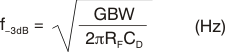
  • Gain-bandwidth (GBW) = 40 MHz

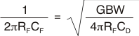
With these three variables set, the feedback capacitor (CF) value can be set to control the frequency response. CF includes the stray capacitance of RF, which is 0.2 pF for a typical surface-mount resistor.

GUID-20220204-SS0I-GCZH-5CVP-WGCB1J8NQPSB-low.svg
NOTE: CF is optional to prevent gain peaking, and includes the stray capacitance of RF.
Figure 7-4 Dual-Supply Transimpedance Amplifier

For an optimized frequency response, use Equation 6 to set the feedback pole:

Equation 6. GUID-40D52EF3-63CB-49DC-89D7-CF6941CCA5F4-low.gif

Equation 7 calculates the bandwidth:

Equation 7. GUID-B413E593-9715-494C-B195-93CD235D1AEB-low.gif

For single-supply applications, the +IN input can be biased with a positive dc voltage to allow the output to reach true zero when the photodiode is not exposed to any light, and respond without the added delay that results from coming out of the negative rail. Figure 7-5 shows this configuration. This bias voltage also appears across the photodiode, providing a reverse bias for faster operation.

GUID-20220204-SS0I-W8CG-ZWWW-ZGTJSLVHNK8Q-low.svg
NOTE: CF is optional to prevent gain peaking, and includes the stray capacitance of RF.
Figure 7-5 Single-Supply Transimpedance Amplifier

For more information, see the Compensate Transimpedance Amplifiers Intuitively application report.