SBOS908A November 2017 – December 2017 OPA2333P
PRODUCTION DATA.
- 1 Features
- 2 Applications
- 3 Description
- 4 Revision History
- 5 Pin Configuration and Functions
- 6 Specifications
- 7 Detailed Description
- 8 Application and Implementation
- 9 Power Supply Recommendations
- 10Layout
- 11Device and Documentation Support
- 12Mechanical, Packaging, and Orderable Information
Package Options
Mechanical Data (Package|Pins)
- DSG|8
Thermal pad, mechanical data (Package|Pins)
- DSG|8
Orderable Information
8 Application and Implementation
NOTE
Information in the following applications sections is not part of the TI component specification, and TI does not warrant its accuracy or completeness. TI’s customers are responsible for determining suitability of components for their purposes. Customers should validate and test their design implementation to confirm system functionality.
8.1 Application Information
The OPA2333P is a unity-gain stable, precision operational amplifier with very low offset voltage drift; these devices are also free from output phase reversal. Applications with noisy or high-impedance power supplies require decoupling capacitors close to the device power-supply pins. In most cases, 0.1-μF capacitors are adequate.
8.2 Typical Application
8.2.1 Bidirectional Current-Sensing
This single-supply, low-side, bidirectional current-sensing solution detects load currents from –1 A to 1 A. The single-ended output spans from 110 mV to 3.19 V. This design uses the OPA2333P because of its low offset voltage and rail-to-rail input and output. One of the amplifiers is configured as a difference amplifier and the other provides the reference voltage.
Figure 23 shows the solution.
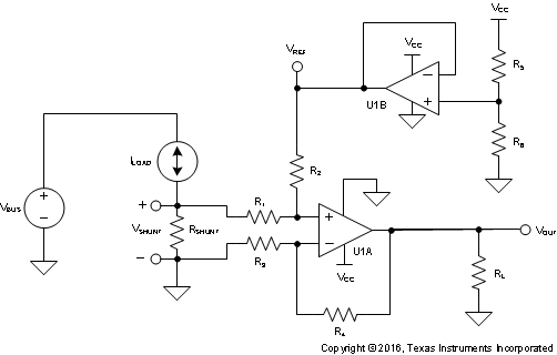 Figure 23. Bidirectional Current-Sensing Schematic
8.2.1.1 Design Requirements
This solution has the following requirements:
- Supply voltage: 3.3 V
- Input: –1 A to 1 A
- Output: 1.65 V ±1.54 V (110 mV to 3.19 V)
8.2.1.2 Detailed Design Procedure
The load current, ILOAD, flows through the shunt resistor (RSHUNT) to develop the shunt voltage, VSHUNT. The shunt voltage is then amplified by the difference amplifier, which consists of U1A and R1 through R4. The gain of the difference amplifier is set by the ratio of R4 to R3. To minimize errors, set R2 = R4 and R1 = R3. The reference voltage, VREF, is supplied by buffering a resistor divider using U1B. The transfer function is given by Equation 1.

where
There are two types of errors in this design: offset and gain. Gain errors are introduced by the tolerance of the shunt resistor and the ratios of R4 to R3 and, similarly, R2 to R1. Offset errors are introduced by the voltage divider (R5 and R6) and how closely the ratio of R4/R3 matches R2/R1. The latter value impacts the CMRR of the difference amplifier, which ultimately translates to an offset error.
Because this is a low-side measurement, the value of VSHUNT is the ground potential for the system load. Therefore, it is important to place a maximum value on VSHUNT. In this design, the maximum value for VSHUNT is set to 100 mV. Equation 2 calculates the maximum value of the shunt resistor given a maximum shunt voltage of 100 mV and maximum load current of 1 A.

The tolerance of RSHUNT is directly proportional to cost. For this design, a shunt resistor with a tolerance of 0.5% was selected. If greater accuracy is required, select a 0.1% resistor or better.
The load current is bidirectional; therefore, the shunt voltage range is –100 mV to 100 mV. This voltage is divided down by R1 and R2 before reaching the operational amplifier, U1A. Take care to ensure that the voltage present at the noninverting node of U1A is within the common-mode range of the device. Therefore, it is important to use an operational amplifier, such as the OPA2333P, that has a common-mode range that extends below the negative supply voltage. Finally, to minimize offset error, note that the OPA2333P has a typical offset voltage of ±2 µV (±10 µV maximum).
Given a symmetric load current of –1 A to 1 A, the voltage divider resistors (R5 and R6) must be equal. To be consistent with the shunt resistor, a tolerance of 0.5% was selected. To minimize power consumption,
10-kΩ resistors were used.
To set the gain of the difference amplifier, the common-mode range and output swing of the OPA2333P must be considered. Equation 3 and Equation 4 depict the typical common-mode range and maximum output swing, respectively, of the OPA2333P given a 3.3-V supply.
The gain of the difference amplifier can now be calculated as shown in Equation 5.

The resistor value selected for R1 and R3 was 1 kΩ. 15.4 kΩ was selected for R2 and R4 because it is the nearest standard value. Therefore, the ideal gain of the difference amplifier is 15.4 V/V.
The gain error of the circuit primarily depends on R1 through R4. As a result of this dependence, 0.1% resistors were selected. This configuration reduces the likelihood that the design requires a two-point calibration. A simple one-point calibration, if desired, removes the offset errors introduced by the 0.5% resistors.
8.2.1.3 Application Curve
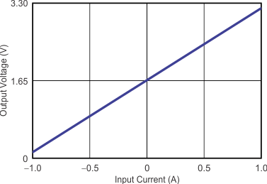
Output Voltage vs Input Current
8.2.2 High-Side Voltage-to-Current (V-I) Converter
The circuit shown in Figure 25 is a high-side voltage-to-current (V-I) converter. It translates to an input voltage of 0 V to 2 V and output current of 0 mA to 100 mA. Figure 26 shows the measured transfer function for this circuit. The low offset voltage and offset drift of the OPA2333P facilitate excellent dc accuracy for the circuit.
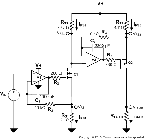 Figure 25. High-Side Voltage-to-Current (V-I) Converter
8.2.2.1 Design Requirements
The design requirements are as follows:
- Supply Voltage: 5 V DC
- Input: 0 V to 2 V DC
- Output: 0 mA to 100 mA DC
8.2.2.2 Detailed Design Procedure
The V-I transfer function of the circuit is based on the relationship between the input voltage, VIN, and the three current sensing resistors, RS1, RS2, and RS3. The relationship between VIN and RS1 determines the current that flows through the first stage of the design. The current gain from the first stage to the second stage is based on the relationship between RS2 and RS3.
For a successful design, pay close attention to the dc characteristics of the operational amplifier chosen for the application. To meet the performance goals, this application benefits from an operational amplifier with low offset voltage, low temperature drift, and rail-to-rail output. The OPA2333P CMOS operational amplifier is a high-precision, 2-uV offset, 0.02-μV/°C drift amplifier optimized for low-voltage, single-supply operation with an output swing to within 50 mV of the positive rail. The OPA2333P family uses chopping techniques to provide low initial offset voltage and near-zero drift over time and temperature. Low offset voltage and low drift reduce the offset error in the system, making these devices appropriate for precise dc control. The rail-to-rail output stage of the OPA2333P ensures that the output swing of the operational amplifier is able to fully control the gate of the MOSFET devices within the supply rails.
A detailed error analysis, design procedure, and additional measured results are given in TIPD102.
8.2.2.3 Application Curve
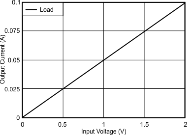 Figure 26. Measured Transfer Function for High-Side V-I Converter
8.2.3 Other Applications
Additional application ideas are shown in Figure 27 and Figure 28.
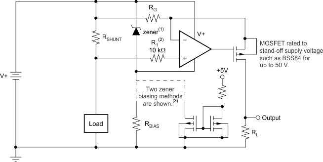
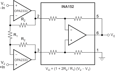 Figure 28. Precision Instrumentation Amplifier


