SBOS908A November   2017  – December 2017 OPA2333P

PRODUCTION DATA.  

  1. Features
  2. Applications
  3. Description
  4. Revision History
  5. Pin Configuration and Functions
  6. Specifications
    1. 6.1 Absolute Maximum Ratings
    2. 6.2 ESD Ratings
    3. 6.3 Recommended Operating Conditions
    4. 6.4 Thermal Information: OPA2333P
    5. 6.5 Electrical Characteristics
    6. 6.6 Typical Characteristics
  7. Detailed Description
    1. 7.1 Overview
    2. 7.2 Functional Block Diagram
    3. 7.3 Feature Description
      1. 7.3.1 Operating Voltage
      2. 7.3.2 Input Voltage
      3. 7.3.3 Internal Offset Correction
      4. 7.3.4 Achieving Output Swing to the Op Amp Negative Rail
      5. 7.3.5 Specified Start-Up Performance
      6. 7.3.6 WSON Package
    4. 7.4 Device Functional Modes
  8. Application and Implementation
    1. 8.1 Application Information
    2. 8.2 Typical Application
      1. 8.2.1 Bidirectional Current-Sensing
        1. 8.2.1.1 Design Requirements
        2. 8.2.1.2 Detailed Design Procedure
        3. 8.2.1.3 Application Curve
      2. 8.2.2 High-Side Voltage-to-Current (V-I) Converter
        1. 8.2.2.1 Design Requirements
        2. 8.2.2.2 Detailed Design Procedure
        3. 8.2.2.3 Application Curve
      3. 8.2.3 Other Applications
  9. Power Supply Recommendations
  10. 10Layout
    1. 10.1 Layout Guidelines
      1. 10.1.1 General Layout Guidelines
      2. 10.1.2 WSON (DFN) Layout Guidelines
    2. 10.2 Layout Example
  11. 11Device and Documentation Support
    1. 11.1 Device Support
      1. 11.1.1 Development Support
    2. 11.2 Documentation Support
      1. 11.2.1 Related Documentation
    3. 11.3 Receiving Notification of Documentation Updates
    4. 11.4 Community Resources
    5. 11.5 Trademarks
    6. 11.6 Electrostatic Discharge Caution
    7. 11.7 Glossary
  12. 12Mechanical, Packaging, and Orderable Information

Package Options

Mechanical Data (Package|Pins)
Thermal pad, mechanical data (Package|Pins)
Orderable Information

Specifications

Absolute Maximum Ratings

over operating free-air temperature range (unless otherwise noted)(1)
MIN MAX UNIT
Supply voltage, VS = (V+) - (V-) Single-supply 7 V
Dual-supply ±3.5
Signal input pins Voltage Common-mode(2) (V–) – 0.3 (V+) + 0.3
Differential(3) ±0.5
Current ±10 mA
Output short current(4) Continuous
Temperature Operating, TA –55 150 °C
Junction, TJ 150
Storage, Tstg –65 150
Stresses beyond those listed under Absolute Maximum Rating may cause permanent damage to the device. These are stress ratings only, which do not imply functional operation of the device at these or any other conditions beyond those indicated under Recommended Operating Conditions. Exposure to absolute-maximum-rated conditions for extended periods may affect device reliability.
Input terminals are diode-clamped to the power-supply rails. Input signals that can swing more than 0.3 V beyond the supply rails must be current-limited to 1 mA or less.
Input terminals are anti-parallel diode-clamped to each other. Input signals that can cause differential voltages of swing more than ±0.5 V must be current-limited to 1 mA or less.
Short-circuit to ground, one amplifier per package.

ESD Ratings

VALUE UNIT
V(ESD) Electrostatic discharge Human body model (HBM), per ANSI/ESDA/JEDEC JS-001, all pins(1) ±4000 V
Charged device model (CDM), per JEDEC specification JESD22-C101, all pins(2) ±1000
JEDEC document JEP155 states that 500-V HBM allows safe manufacturing with a standard ESD control process.
JEDEC document JEP157 states that 250-V CDM allows safe manufacturing with a standard ESD control process. 

Recommended Operating Conditions

over operating free-air temperature range (unless otherwise noted)
MIN NOM MAX UNIT
VS Supply voltage, [ (V+) – (V–) ] Single supply 1.8 5.5 V
Dual supply ±0.9 ±2.75
Specified temperature –40 125 °C

Thermal Information: OPA2333P

THERMAL METRIC(1) OPA2333P UNIT
DSG (WSON)
8 PINS
RθJA Junction-to-ambient thermal resistance 74.5 °C/W
RθJC(top) Junction-to-case (top) thermal resistance 93.5 °C/W
RθJB Junction-to-board thermal resistance 41.1 °C/W
ΨJT Junction-to-top characterization parameter 4.3 °C/W
ΨJB Junction-to-board characterization parameter 41.2 °C/W
RθJC(bot) Junction-to-case (bottom) thermal resistance 15.7 °C/W
For more information about traditional and new thermal metrics, see the Semiconductor and IC Package Thermal Metrics application report.

Electrical Characteristics

At TA = 25°C, RL= 10 kΩ connected to VS / 2, VCM = VS / 2, and VOUT = VS / 2 (unless otherwise noted)
PARAMETER TEST CONDITIONS MIN TYP MAX UNIT
OFFSET VOLTAGE
VOS Input offset voltage VS = 5 V ±2 ±10 µV
dVOS/dT Input offset voltage drift VS = 5 V TA = –40°C to +125°C 0.02 ±0.05 µV/°C
PSRR Power-supply rejection ratio 1.8 V ≤ VS ≤ 5.5 V TA = –40°C to +125°C 1 ±5 µV/V
Channel separation, dc 0.1 µV/V
INPUT BIAS CURRENT
IB Input bias current ±70 ±200 pA
TA = –40°C to +125°C ±150 pA
IOS Input offset current ±140 ±400 pA
NOISE
EN Input voltage noise f = 0.1 Hz to 10 Hz, peak-to-peak 1.1 µVPP
f = 0.1 Hz to 10 Hz, RMS 0.2 µVRMS
eN Input voltage noise density f = 10 Hz 55 nV/√Hz
f = 1 kHz 55 nV/√Hz
iN Input current noise density f = 10 Hz 100 fA/√Hz
INPUT VOLTAGE
VCM Common-mode voltage range (V–) – 0.1 (V+) + 0.1 V
CMRR Common-mode rejection ratio (V–) – 0.1 V ≤ VCM ≤ (V+) + 0.1 V, VS = 5.5 V 106 130 dB
INPUT IMPEDANCE
ZID Differential 1013 || 2 Ω || pF
ZICM Common-mode 1013 || 4 Ω || pF
OPEN-LOOP GAIN
AOL Open-loop voltage gain TA = –40°C to +125°C (V–) + 100 mV ≤ VO ≤ (V+) – 100 mV, RL = 10 kΩ 106 130 dB
FREQUENCY RESPONSE
φm Phase margin VO = 10 mVPP 65 Degrees
GBW Gain-bandwidth product VO = 10 mVPP 350 kHz
SR Slew rate VO = 4-V step G = 1 0.16 V/µs
OUTPUT
Output voltage swing 30 50 mV
TA = –40°C to +125°C 70 mV
ISC Short-circuit current ±5 mA
CL Capactive load drive See Typical Characteristics
ZO Open-loop output impedance f = 350 kHz, IO = 0 mA 2
Start-up time VS = 5 V 100 500 µs
POWER SUPPLY
VS Specified voltage 1.8 5.5 V
IQ Quiescent current (per amplifier) IO = 0 A 17 25 µA
TA = –40°C to +125°C 28
TEMPERATURE RANGE
TA Specified range –40 125 °C
TA Operating range –55 150 °C

Typical Characteristics

Table 1. List of Typical Characteristics

TITLE FIGURE
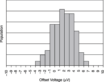
Offset Voltage Production Distribution Figure 1
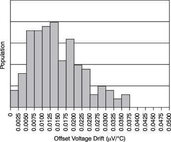
Offset Voltage Drift Production Distribution Figure 2
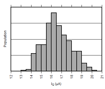
Quiescent Current Production Distribution Figure 3
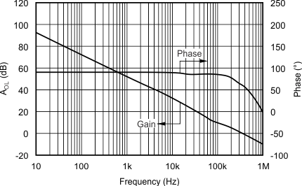
Open-Loop Gain vs Frequency Figure 4
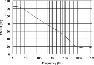
Common-Mode Rejection Ratio vs Frequency Figure 5
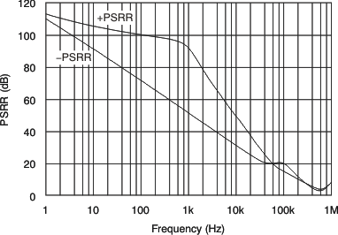
Power-Supply Rejection Ratio vs Frequency Figure 6
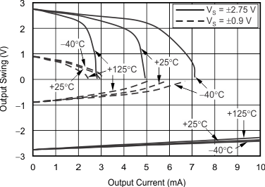
Output Voltage Swing vs Output Current Figure 7
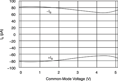
Input Bias Current vs Common-Mode Voltage Figure 8
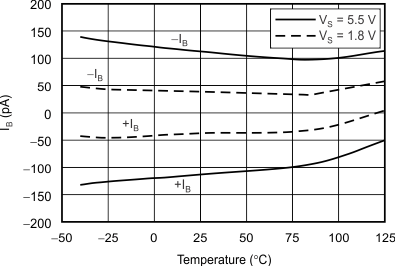
Input Bias Current vs Temperature Figure 9
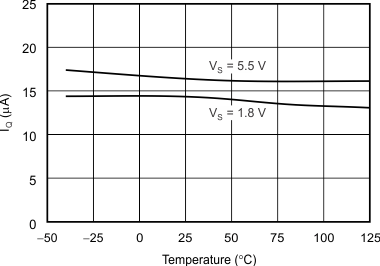
Quiescent Current vs Temperature Figure 10
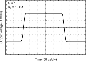
Large-Signal Step Response Figure 11
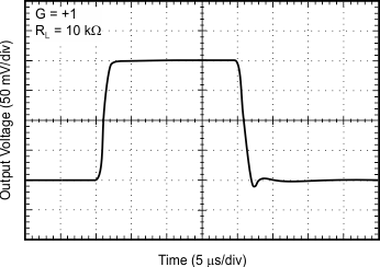
Small-Signal Step Response Figure 12
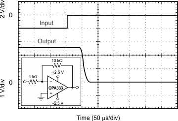
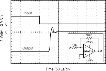
Positive Overvoltage Recovery Figure 13
Negative Overvoltage Recovery Figure 14
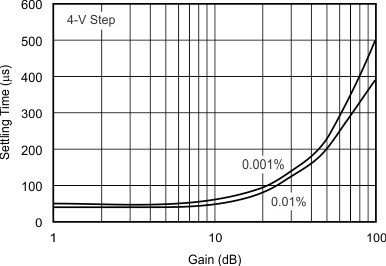
Settling Time vs Closed-Loop Gain Figure 15
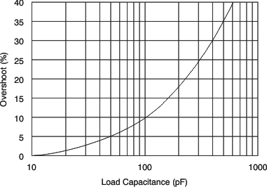
Small-Signal Overshoot vs Load Capacitance Figure 16
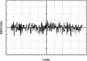
0.1-Hz to 10-Hz Noise Figure 17
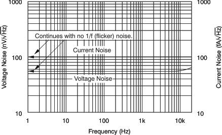
Current and Voltage Noise Spectral Density vs Frequency Figure 18
At TA = 25°C, VS = 5 V, and CL = 0 pF, unless otherwise noted.
OPA2333P tc_histo_bos351.gif
Figure 1. Offset Voltage Production Distribution
OPA2333P tc_histo_drift_bos351.gif
Figure 2. Offset Voltage Drift Production Distribution
OPA2333P Iq_data_hist.gif
VS = 5.5 V
Figure 3. Quiescent Current Production Distribution
OPA2333P tc_cmrr-frq_bos351.gif
Figure 5. Common-Mode Rejection Ratio vs Frequency
OPA2333P tc_vos-io_bos351.gif
Figure 7. Output Voltage Swing vs Output Current
OPA2333P tc_ib-tmp_bos351.gif
Figure 9. Input Bias Current vs Temperature
OPA2333P tc_resp_lg_bos351.gif
Figure 11. Large-Signal Step Response
OPA2333P tc_pos_recov_bos351.gif
Figure 13. Positive Overvoltage Recovery
OPA2333P tc_tim-cloop_bos351.gif
Figure 15. Settling Time vs Closed-Loop Gain
OPA2333P tc_noise_bos351.gif
Figure 17. 0.1-Hz to 10-Hz Noise
OPA2333P tc_oloop-frq_bos351.gif
Figure 4. Open-Loop Gain and Phase vs Frequency
OPA2333P tc_psrr-frq_bos351.gif
Figure 6. Power-Supply Rejection Ratio vs Frequency
OPA2333P tc_ib-vcm_bos351.gif
Figure 8. Input Bias Current vs Common-Mode Voltage
OPA2333P tc_iq-tmp_bos351.gif
Figure 10. Quiescent Current vs Temperature
OPA2333P tc_resp_sm_bos351.gif
Figure 12. Small-Signal Step Response
OPA2333P tc_neg_recov_bos351.gif
Figure 14. Negative Overvoltage Recovery
OPA2333P tc_ovrshoot-cl_bos351.gif
Figure 16. Small-Signal Overshoot
vs Load Capacitance
OPA2333P tc_noise-frq_bos351.gif
Figure 18. Current and Voltage Noise Spectral Density vs Frequency