SBOS365G may   2006  – may 2023 OPA2365 , OPA365

PRODUCTION DATA  

  1.   1
  2. Features
  3. Applications
  4. Description
  5. Revision History
  6. Device Comparison Table
  7. Pin Configuration and Functions
  8. Specifications
    1. 7.1 Absolute Maximum Ratings
    2. 7.2 ESD Ratings
    3. 7.3 Recommended Operating Conditions
    4. 7.4 Thermal Information: OPA365
    5. 7.5 Thermal Information: OPA2365
    6. 7.6 Electrical Characteristics
    7. 7.7 Typical Characteristics
  9. Detailed Description
    1. 8.1 Overview
    2. 8.2 Functional Block Diagram
    3. 8.3 Feature Description
      1. 8.3.1 Rail-to-Rail Input
      2. 8.3.2 Input and ESD Protection
      3. 8.3.3 Capacitive Loads
      4. 8.3.4 Achieving an Output Level of Zero Volts (0 V)
      5. 8.3.5 Active Filtering
    4. 8.4 Device Functional Modes
  10. Application and Implementation
    1. 9.1 Application Information
      1. 9.1.1 Basic Amplifier Configurations
    2. 9.2 Typical Application
      1. 9.2.1 Design Requirements
      2. 9.2.2 Detailed Design Procedure
      3. 9.2.3 Application Curve
    3. 9.3 System Examples
      1. 9.3.1 Driving an Analog-to-Digital Converter
    4. 9.4 Power Supply Recommendations
    5. 9.5 Layout
      1. 9.5.1 Layout Guidelines
      2. 9.5.2 Layout Example
  11. 10Device and Documentation Support
    1. 10.1 Device Support
      1. 10.1.1 Development Support
        1. 10.1.1.1 PSpice® for TI
        2. 10.1.1.2 TINA-TI™ Simulation Software (Free Download)
        3. 10.1.1.3 DIP-Adapter-EVM
        4. 10.1.1.4 DIYAMP-EVM
        5. 10.1.1.5 TI Reference Designs
        6. 10.1.1.6 Filter Design Tool
    2. 10.2 Documentation Support
      1. 10.2.1 Related Documentation
    3. 10.3 Receiving Notification of Documentation Updates
    4. 10.4 Support Resources
    5. 10.5 Trademarks
    6. 10.6 Electrostatic Discharge Caution
    7. 10.7 Glossary
  12. 11Mechanical, Packaging, and Orderable Information

Package Options

Mechanical Data (Package|Pins)
Thermal pad, mechanical data (Package|Pins)
Orderable Information

Basic Amplifier Configurations

As with other single-supply op amps, the OPAx365 can be operated with either a single supply or dual supplies. Figure 9-1 shows a typical dual-supply connection, which is accompanied by a single-supply connection. The OPAx365 are configured as a basic inverting amplifier with a gain of −10 V/V. The dual-supply connection has an output voltage centered on zero, while the single-supply connection has an output centered on the common-mode voltage VCM. For the circuit shown, this voltage is 1.5 V, but can be any value within the common-mode input voltage range. The OPAx365 VCM range extends 100 mV beyond the power-supply rails.
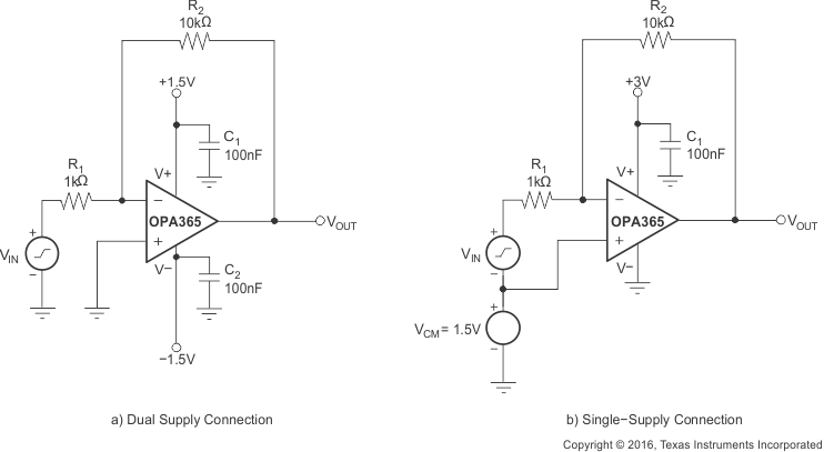
GUID-947FE2B8-651E-46D9-A044-38042E4BAD00-low.gifFigure 9-1 Basic Circuit Connections

Figure 9-2 shows a single-supply, electret microphone application where VCM is provided by a resistive divider. The divider also provides the bias voltage for the electret element.
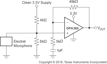
GUID-E1904E6A-F9E3-4492-BFF3-E59EE28A48C2-low.gifFigure 9-2 Microphone Preamplifier