SBOS538F January 2011 – December 2016 OPA2322 , OPA322 , OPA4322
PRODUCTION DATA.
- 1 Features
- 2 Applications
- 3 Description
- 4 Revision History
- 5 Pin Configuration and Functions
- 6 Specifications
- 7 Detailed Description
- 8 Application and Implementation
- 9 Power Supply Recommendations
- 10Layout
- 11Device and Documentation Support
- 12Mechanical, Packaging, and Orderable Information
Package Options
Mechanical Data (Package|Pins)
Thermal pad, mechanical data (Package|Pins)
Orderable Information
6 Specifications
6.1 Absolute Maximum Ratings
over operating free-air temperature range (unless otherwise noted)(1)| MIN | MAX | UNIT | ||
|---|---|---|---|---|
| Voltage | Supply voltage, VS = (V+) – (V–) | 6 | V | |
| Signal input pins(2) | (V–) – 0.5 | (V+) + 0.5 | V | |
| Current | Signal input pins(2) | –10 | 10 | mA |
| Output short-circuit(3) | Continuous | |||
| Temperature | Operating, TA | –40 | 150 | °C |
| Junction, TJ | 150 | °C | ||
| Storage, Tstg | –65 | 150 | °C | |
(1) Stresses beyond those listed under Absolute Maximum Ratings may cause permanent damage to the device. These are stress ratings only, which do not imply functional operation of the device at these or any other conditions beyond those indicated under Recommended Operating Conditions. Exposure to absolute-maximum-rated conditions for extended periods may affect device reliability.
(2) Input terminals are diode-clamped to the power-supply rails. Input signals that can swing more than 0.5 V beyond the supply rails must be current limited to 10 mA or less.
(3) Short-circuit to ground, one amplifier per package.
6.2 ESD Ratings
| VALUE | UNIT | |||
|---|---|---|---|---|
| V(ESD) | Electrostatic discharge | Human-body model (HBM), per ANSI/ESDA/JEDEC JS-001(1) | ±4000 | V |
| Charged-device model (CDM), per JEDEC specification JESD22-C101(2) | ±1000 | |||
| Machine model (MM) | ±200 | |||
(1) JEDEC document JEP155 states that 500-V HBM allows safe manufacturing with a standard ESD control process.
(2) JEDEC document JEP157 states that 250-V CDM allows safe manufacturing with a standard ESD control process.
6.3 Recommended Operating Conditions
over operating free-air temperature range (unless otherwise noted)| MIN | MAX | UNIT | ||
|---|---|---|---|---|
| VS | Specified voltage | 1.8 | 5.5 | V |
| TA | Specified temperature | –40 | 125 | °C |
6.4 Thermal Information: OPA322, OPA322S
| THERMAL METRIC(1) | OPA322 | OPA322S | UNITS | |
|---|---|---|---|---|
| DBV (SOT-23) | DBV (SOT-23) | |||
| 5 PINS | 6 PINS | |||
| RθJA | Junction-to-ambient thermal resistance | 219.3 | 177.5 | °C/W |
| RθJC(top) | Junction-to-case(top) thermal resistance | 107.5 | 108.9 | °C/W |
| RθJB | Junction-to-board thermal resistance | 57.5 | 27.4 | °C/W |
| ψJT | Junction-to-top characterization parameter | 7.4 | 13.3 | °C/W |
| ψJB | Junction-to-board characterization parameter | 56.9 | 26.9 | °C/W |
| RθJC(bot) | Junction-to-case(bottom) thermal resistance | — | — | °C/W |
(1) For more information about traditional and new thermal metrics, see the Semiconductor and IC Package Thermal Metrics application report.
6.5 Thermal Information: OPA2322, OPA2322S
| THERMAL METRIC(1) | OPA2322 | OPA2322S | UNITS | |||
|---|---|---|---|---|---|---|
| D (SOIC) | DRG (SON) | DGK (VSSOP) | DGS (VSSOP) | |||
| 8 PINS | 8 PINS | 8 PINS | 10 PINS | |||
| RθJA | Junction-to-ambient thermal resistance | 122.6 | 50.6 | 174.8 | 171.5 | °C/W |
| RθJC(top) | Junction-to-case(top) thermal resistance | 67.1 | 54.9 | 43.9 | 43 | °C/W |
| RθJB | Junction-to-board thermal resistance | 64 | 25.2 | 95 | 91.4 | °C/W |
| ψJT | Junction-to-top characterization parameter | 13.2 | 0.6 | 2 | 1.9 | °C/W |
| ψJB | Junction-to-board characterization parameter | 63.4 | 25.3 | 93.5 | 89.9 | °C/W |
| RθJC(bot) | Junction-to-case(bottom) thermal resistance | — | 5.7 | — | — | °C/W |
(1) For more information about traditional and new thermal metrics, see the Semiconductor and IC Package Thermal Metrics application report.
6.6 Thermal Information: OPA4322, OPA4322S
| THERMAL METRIC(1) | OPA4322 | OPA4322S | UNITS | |
|---|---|---|---|---|
| PW (TSSOP) | PW (TSSOP) | |||
| 14 PINS | 16 PINS | |||
| RθJA | Junction-to-ambient thermal resistance | 109.8 | 105.9 | °C/W |
| RθJC(top) | Junction-to-case(top) thermal resistance | 34.9 | 28.1 | °C/W |
| RθJB | Junction-to-board thermal resistance | 52.5 | 51.1 | °C/W |
| ψJT | Junction-to-top characterization parameter | 2.2 | 0.8 | °C/W |
| ψJB | Junction-to-board characterization parameter | 51.8 | 50.4 | °C/W |
| RθJC(bot) | Junction-to-case(bottom) thermal resistance | — | — | °C/W |
(1) For more information about traditional and new thermal metrics, see the Semiconductor and IC Package Thermal Metrics application report.
6.7 Electrical Characteristics
At VS = 1.8 V to 5.5 V, or ±0.9 V to ±2.75 V, TA = 25°C, RL = 10 kΩ connected to VS/2, VCM = VS/2, VOUT = VS/2, andSHDN_x = VS+ (unless otherwise noted).
| PARAMETER | TEST CONDITIONS | MIN | TYP | MAX | UNIT | |||
|---|---|---|---|---|---|---|---|---|
| OFFSET VOLTAGE | ||||||||
| VOS | Input offset voltage | 0.5 | 2 | mV | ||||
| dVOS/dT | vs temperature | VS = 5.5 V | 1.8 | 6 | μV/°C | |||
| PSR | vs power supply | VS = 1.8 V to 5.5 V | TA = 25°C | 10 | 50 | μV/V | ||
| TA = –40°C to 125°C | 20 | 65 | ||||||
| Channel separation | At 1 kHz | 130 | dB | |||||
| INPUT VOLTAGE | ||||||||
| VCM | Common-mode voltage range | (V–) – 0.1 | (V+) + 0.1 | V | ||||
| CMRR | Common-mode rejection ratio | (V–) – 0.1 V < VCM < (V+) + 0.1 V | TA = 25°C | 90 | 100 | dB | ||
| TA = –40°C to 125°C | 90 | |||||||
| INPUT BIAS CURRENT | ||||||||
| IB | Input bias current | TA = 25°C | ±0.2 | ±10 | pA | |||
| TA = –40°C to 85°C | ±50 | |||||||
| OPA322 and OPA322S, TA = –40°C to 125°C | ±800 | |||||||
| OPA2322 and OPA2322S, TA = –40°C to 125°C | ±400 | |||||||
| OPA4322 and OPA4322S, TA = –40°C to 125°C | ±400 | |||||||
| IOS | Input offset current | TA = 25°C | ±0.2 | ±10 | pA | |||
| TA = –40°C to 85°C | ±50 | |||||||
| TA = –40°C to 125°C | ±400 | |||||||
| NOISE | ||||||||
| Input voltage noise | f = 0.1 Hz to 10 Hz | 2.8 | μVPP | |||||
| en | Input voltage noise density | f = 1 kHz | 8.5 | nV/√Hz | ||||
| f = 10 kHz | 7 | |||||||
| in | Input current noise density | f = 1 kHz | 0.6 | fA/√Hz | ||||
| INPUT CAPACITANCE | ||||||||
| Differential | 5 | pF | ||||||
| Common-mode | 4 | pF | ||||||
| OPEN-LOOP GAIN | ||||||||
| AOL | Open-loop voltage gain | 0.1 V < VO < (V+) – 0.1 V, RL = 10 kΩ | 100 | 130 | dB | |||
| 0.1 V < VO < (V+) – 0.1 V, RL = 10 kΩ | 94 | |||||||
| PM | Phase margin | VS = 5 V, CL = 50 pF | 47 | ° | ||||
| FREQUENCY RESPONSE | ||||||||
| GBP | Gain bandwidth product | VS = 5 V, CL = 50 pF, unity gain | 20 | MHz | ||||
| SR | Slew rate | VS = 5 V, CL = 50 pF, G = +1 | 10 | V/μs | ||||
| tS | Settling time | VS = 5 V, CL = 50 pF, to 0.1%, 2-V step, G = +1 | 0.25 | μs | ||||
| VS = 5 V, CL = 50 pF, to 0.01%, 2-V step, G = +1 | 0.32 | |||||||
| Overload recovery time | VS = 5 V, CL = 50 pF, VIN × G > VS | 100 | ns | |||||
| THD+N | Total harmonic distortion + noise(1) | VS = 5 V, CL = 50 pF, VO = 4 VPP, G = +1, f = 10 kHz, RL = 10 kΩ |
0.0005% | |||||
| VS = 5 V, CL = 50 pF, VO = 2 VPP, G = +1, f = 10 kHz, RL = 600 Ω |
0.0011% | |||||||
| OUTPUT | ||||||||
| VO | Voltage output (swing from both rails) | RL = 10 kΩ | TA = 25°C | 10 | 20 | mV | ||
| TA = –40°C to 125°C | 30 | |||||||
| ISC | Short-circuit current | VS = 5.5 V | ±65 | mA | ||||
| CL | Capacitive load drive | See Typical Characteristics | ||||||
| RO | Open-loop output resistance | IO = 0 mA, f = 1 MHz | 90 | Ω | ||||
| POWER SUPPLY | ||||||||
| VS | Specified voltage range | 1.8 | 5.5 | V | ||||
| IQ | Quiescent current per amplifier | OPA322 and OPA322S, IO = 0 mA, VS = 5.5 V |
TA = 25°C | 1.6 | 1.9 | mA | ||
| TA = –40°C to 125°C | 2 | |||||||
| OPA2322 and OPA2322S, IO = 0 mA, VS = 5.5 V |
TA = 25°C | 1.5 | 1.75 | |||||
| TA = –40°C to 125°C | 1.85 | |||||||
| OPA4322 and OPA4322S, IO = 0 mA, VS = 5.5 V |
TA = 25°C | 1.4 | 1.65 | |||||
| TA = –40°C to 125°C | 1.75 | |||||||
| Power-on time | VS+ = 0 V to 5 V, to 90% IQ level | 28 | μs | |||||
| SHUTDOWN(2) | ||||||||
| IQSD | Quiescent current (per amplifier) |
VS = 1.8 V to 5.5 V, all amplifiers disabled, SHDN = VS– | 0.1 | 0.5 | µA | |||
| VIH | High voltage (enabled) | VS = 1.8 V to 5.5 V, amplifier enabled | (V+) – 0.1 | V | ||||
| VIL | Low voltage (disabled) | VS = 1.8 V to 5.5 V, amplifier disabled | (V–) + 0.1 | V | ||||
| tON | Amplifier enable time (full shutdown)(3) |
VS = 1.8 V to 5.5 V, full shutdown; G = 1, VOUT = 0.9 × VS/2(4) |
10 | µs | ||||
| Amplifier enable time (partial shutdown)(3) |
VS = 1.8 V to 5.5 V, partial shutdown; G = 1, VOUT = 0.9 × VS/2(4) |
6 | µs | |||||
| tOFF | Amplifier disable time(3) | VS = 1.8 V to 5.5 V, G = 1, VOUT = 0.1 × VS/2 | 3 | µs | ||||
| SHDN pin input bias current (per pin) |
VS = 1.8 V to 5.5 V, VIH = 5 V | 0.13 | µA | |||||
| VS = 1.8 V to 5.5 V, VIL = 0 V | 0.04 | |||||||
(1) Third-order filter; bandwidth = 80 kHz at –3 dB
(2) Ensured by design and characterization; not production tested.
(3) Disable time (tOFF) and enable time (tON) are defined as the time interval between the 50% point of the signal applied to the SHDN pin and the point at which the output voltage reaches the 10% (disable) or 90% (enable) level.
(4) Full shutdown refers to the dual OPA2322S having both channels A and B disabled (SHDN_A = SHDN_B = VS–) and the quad OPA4322S having all channels A to D disabled (SHDN_A/B = SHDN_C/D = VS–). For partial shutdown, only one SHDN pin is exercised; in this mode, the internal biasing and oscillator remain operational and the enable time is shorter.
6.8 Typical Characteristics
At TA = 25°C, VCM = VOUT = mid-supply, and RL = 10 kΩ (unless otherwise noted).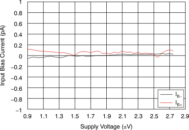 Figure 3. Input Bias Current vs Supply Voltage
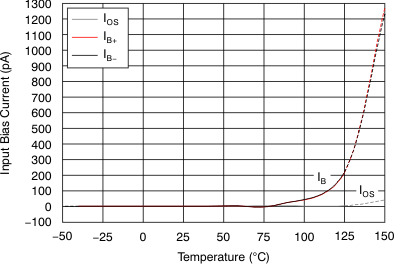 Figure 5. Input Bias Current vs Temperature
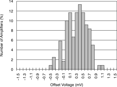 Figure 7. Offset Voltage Production Histogram
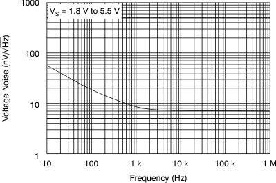 Figure 9. Input Voltage Noise Spectral Density
vs Frequency
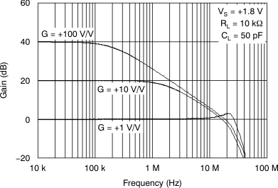 Figure 11. Closed-Loop Gain vs Frequency
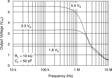 Figure 13. Maximum Output Voltage vs Frequency
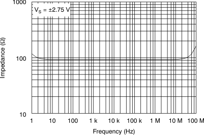 Figure 15. Open-Loop Output Impedance
vs Frequency
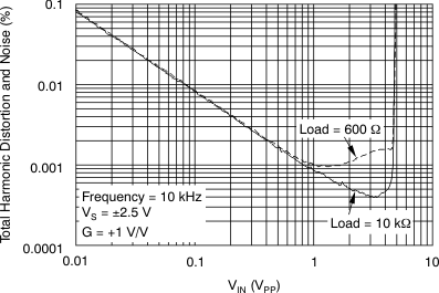 Figure 17. THD+N vs Amplitude
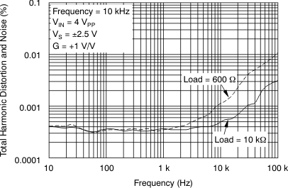 Figure 19. THD+N vs Frequency
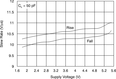 Figure 21. Slew Rate vs Supply Voltage
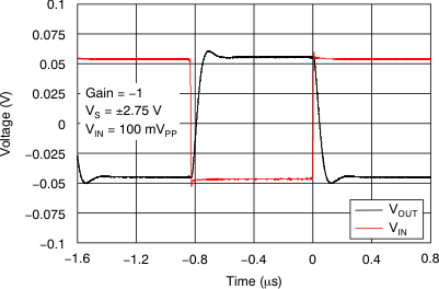 Figure 23. Small-Signal Step Response
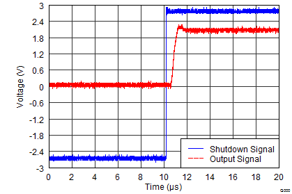 Figure 27. Turnon Transient
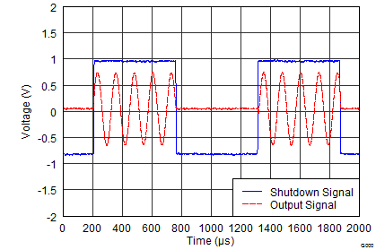
1.8 V (Low Supply)
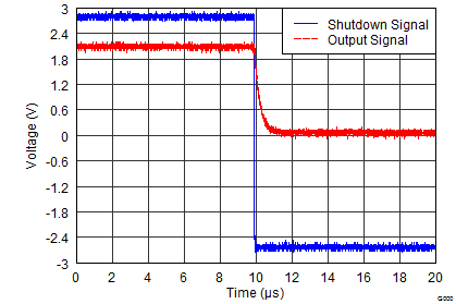
Figure 29. Turnon and Turnoff Transient
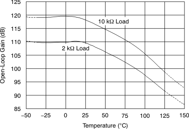 Figure 2. Open-Loop Gain vs Temperature
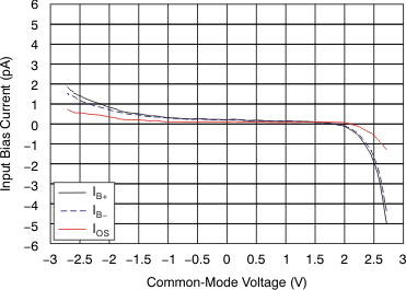 Figure 4. Input Bias Current
vs Common-Mode Voltage
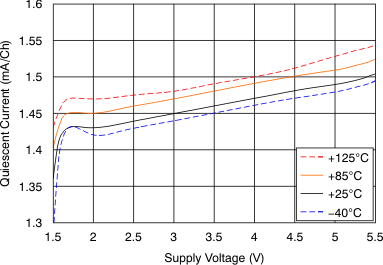 Figure 6. Quiescent Current vs Supply Voltage
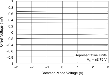 Figure 8. Offset Voltage vs Common-Mode Voltage
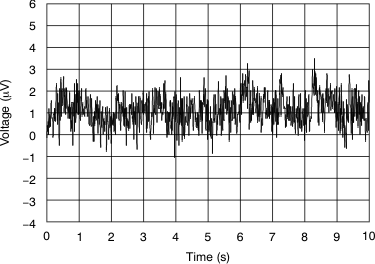 Figure 10. 0.1-Hz to 10-Hz Input Voltage Noise
 Figure 12. Closed-Loop Gain vs Frequency
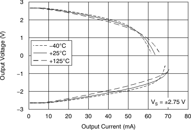 Figure 14. Output Voltage Swing vs Output Current
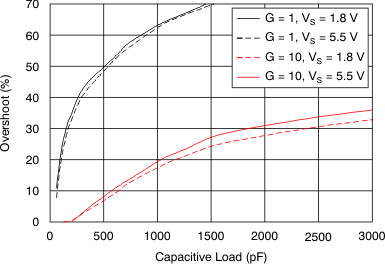 Figure 16. Small-Signal Overshoot
vs Load Capacitance
 Figure 18. THD+N vs Frequency
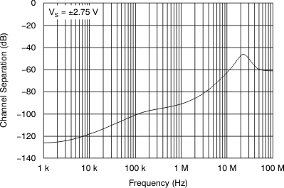 Figure 20. Channel Separation
vs Frequency (for Dual)
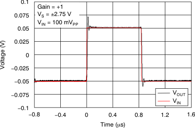 Figure 22. Small-Signal Step Response
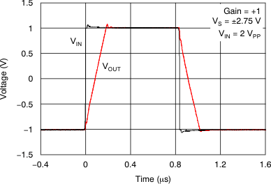 Figure 24. Large-Signal Step Response vs Time
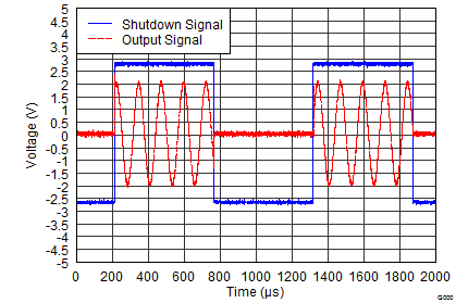
5.5 V (High Supply)
Figure 28. Turnon and Turnoff Transient
