SBOS099D September 2000 – December 2015 OPA2350 , OPA350 , OPA4350
PRODUCTION DATA.
- 1 Features
- 2 Applications
- 3 Description
- 4 Revision History
- 5 Pin Configuration and Functions
- 6 Specifications
- 7 Detailed Description
-
8 Application and Implementation
- 8.1 Application Information
- 8.2 Typical Applications
- 9 Power Supply Recommendations
- 10Layout
- 11Device and Documentation Support
- 12Mechanical, Packaging, and Orderable Information
Package Options
Mechanical Data (Package|Pins)
Thermal pad, mechanical data (Package|Pins)
Orderable Information
8 Application and Implementation
NOTE
Information in the following applications sections is not part of the TI component specification, and TI does not warrant its accuracy or completeness. TI’s customers are responsible for determining suitability of components for their purposes. Customers should validate and test their design implementation to confirm system functionality.
8.1 Application Information
Low pass filters are commonly employed in signal processing applications to reduce noise and prevent aliasing. The OPAx350 are ideally suited to construct high speed, high precision active filters. Figure 29 illustrates a second order low pass filter commonly encountered in signal processing applications.
8.2 Typical Applications
8.2.1 Second Order Low Pass Filter
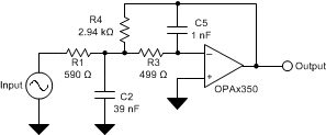 Figure 29. Second Order Low Pass Filter
8.2.1.1 Design Requirements
Use the following parameters for this design example:
- Gain = 5 V/V (inverting gain).
- Low pass cutoff frequency = 25 kHz.
- Second order Chebyshev filter response with 3-dB gain peaking in the passband.
8.2.1.2 Detailed Design Procedure
The infinite-gain multiple-feedback circuit for a low-pass network function is shown in Equation 1. Use Equation 2 to calculate the voltage transfer function.

This circuit produces a signal inversion. For this circuit the gain at DC and the low pass cutoff frequency can be calculated using Equation 2.

Software tools are readily available to simplify filter design. WEBENCH® Filter Designer is a simple, powerful, and easy-to-use active filter design program. The WEBENCH Filter Designer lets you create optimized filter designs using a selection of TI operational amplifiers and passive components from TI's vendor partners. Available as a web based tool from the WEBENCH® Design Center, WEBENCH® Filter Designer allows you to design, optimize, and simulate complete multi-stage active filter solutions within minutes.
8.2.1.3 Application Curve
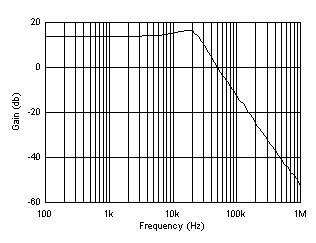 Figure 30. OPAx350 2nd Order 25-kHz, Chebyshev, Low-Pass Filter
8.2.2 Single-Supply Video Line Driver
Figure 31 shows a circuit for a single supply, G = 2 composite video line driver. The synchronized outputs of a composite video line driver extend below ground. As shown, the input to the operational amplifier should be AC-coupled and shifted positively to provide adequate signal swing to account for these negative signals in a single-supply configuration.
The input is terminated with a 75-Ω resistor and AC-coupled with a 47-μF capacitor to a voltage divider that provides the DC bias point to the input. In Figure 31, this point is approximately (V−) + 1.7 V. Setting the optimal bias point requires some understanding of the nature of composite video signals. For best performance, avoid the distortion caused by the transition region of the complementary input stage of the OPA350. See the discussion of rail-to-rail input in Rail-to-Rail Input.
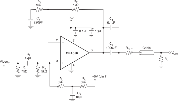 Figure 31. Single-Supply Video Line Driver
8.2.3 Adding a Feedback Capacitor to Improve Response
For optimum settling time and stability with high-impedance feedback networks, it may be necessary to add a feedback capacitor across the feedback resistor, RF, as shown in Figure 32. This capacitor compensates for the zero created by the feedback network impedance and the input capacitance of the OPA350 (and any parasitic layout capacitance). The effect becomes more significant with higher impedance networks.
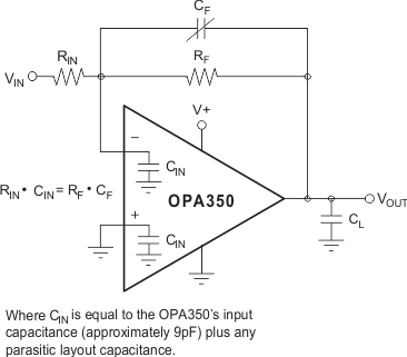 Figure 32. Feedback Capacitor Improves Dynamic Performance
A variable capacitor can be used for the feedback capacitor, because input capacitance may vary between operational amplifiers and layout capacitance is difficult to determine. For the circuit shown in Figure 32, the value of the variable feedback capacitor should be chosen so that the input resistance times the input capacitance of the OPA350 (typically 9 pF) plus the estimated parasitic layout capacitance equals the feedback capacitor times the feedback resistor:
where
- CIN is equal to the input capacitance of the OPA350 (sum of differential and common-mode) plus the layout capacitance.
The capacitor can be varied until optimum performance is obtained.
8.2.4 Two Op-Amp Instrumentation Amplifier With Improved High-Frequency Common-Mode Rejection
The OPAx350 is well suited for high input impedance applications such as an instrumentation amplifier. The two amplifier configuration shown in Figure 33 rejects any common mode signals and senses the small differential input voltage developed by the resistive bridge. The voltage reference sets the output to 2.5 V when the differential signal developed by the bridge is zero. The high common mode rejection versus frequency response of the OPAx350, rejects and common mode noise that may be coupled into the bridge circuit from the bridge excitation source. The gain of the circuit is determined by RG according to the equation shown in Figure 33.
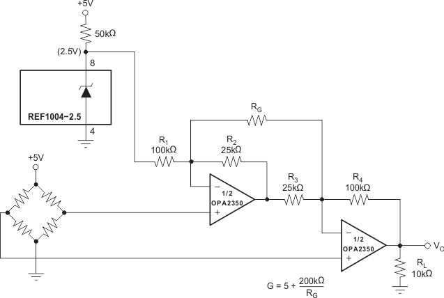 Figure 33. Two Op-Amp Instrumentation Amplifier With Improved High-Frequency Common-Mode Rejection Schematic
8.2.5 10-kHz High-Pass Filter
High-pass filters are used to reject DC signals and low-frequency time varying signals such as drift versus temperature. Figure 34 illustrates a high-pass filter with a 10 kHz low-frequency cutoff frequency.
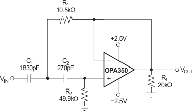 Figure 34. 10-kHz High-Pass Filter