SBOS432G August 2008 – August 2016 OPA2330 , OPA330 , OPA4330
PRODUCTION DATA.
- 1 Features
- 2 Applications
- 3 Description
- 4 Revision History
- 5 Device Comparison Table
- 6 Pin Configurations and Functions
- 7 Specifications
- 8 Detailed Description
- 9 Application and Implementation
- 10Power Supply Recommendations
- 11Layout
- 12Device and Documentation Support
- 13Mechanical, Packaging, and Orderable Information
Package Options
Refer to the PDF data sheet for device specific package drawings
Mechanical Data (Package|Pins)
- D|14
- RGY|14
- PW|14
Thermal pad, mechanical data (Package|Pins)
- RGY|14
Orderable Information
8 Detailed Description
8.1 Overview
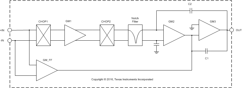
The OPA330 family of Zerø-Drift amplifiers feature a proprietary auto-calibration technique to simultaneously achieve near-zero drift over time and temperature at only 35 µA (maximum) of quiescent current while also providing low offset voltage (50 µV maximum). These devices are unity-gain stable, precision operational amplifiers free from unexpected output and phase reversal. The OPA330 series are also optimized for low-voltage, single-supply operation: as low as 1.8 V (±0.9 V) and up to 5.5 V (±2.75 V).
The proprietary Zerø-Drift circuitry lowers the 1/f noise component as well as offers the advantage of low input offset voltage over time and temperature. The OPA330 series of operational amplifiers are ideal for cost-sensitive applications and applications that operate without regulation directly from battery power.
8.2 Functional Block Diagram

8.3 Feature Description
The OPA33x family is unity-gain stable and free from unexpected output phase reversal. These devices use a proprietary auto-calibration technique to provide low offset voltage and very low drift over time and temperature. For lowest offset voltage and precision performance, optimize circuit layout, and mechanical conditions. Avoid temperature gradients that create thermoelectric (Seebeck) effects in the thermocouple junctions formed from connecting dissimilar conductors. Cancel these thermally-generated potentials by assuring they are equal on both input terminals. Other layout and design considerations include:
- Use low thermoelectric-coefficient conditions (avoid dissimilar metals).
- Thermally isolate components from power supplies or other heat sources.
- Shield operational amplifier and input circuitry from air currents, such as cooling fans.
Following these guidelines reduces the likelihood of junctions being at different temperatures, which can cause thermoelectric voltage drift of 0.1 µV/°C or higher, depending on materials used.
8.4 Device Functional Modes
The OPAx330 has a single functional mode and is operational when the power-supply voltage is greater than
1.8 V (±0.9 V). The maximum power-supply voltage for the OPAx330 is 5.5 V (±2.75 V).