SBOS432G August 2008 – August 2016 OPA2330 , OPA330 , OPA4330
PRODUCTION DATA.
- 1 Features
- 2 Applications
- 3 Description
- 4 Revision History
- 5 Device Comparison Table
- 6 Pin Configurations and Functions
- 7 Specifications
- 8 Detailed Description
- 9 Application and Implementation
- 10Power Supply Recommendations
- 11Layout
- 12Device and Documentation Support
- 13Mechanical, Packaging, and Orderable Information
Package Options
Refer to the PDF data sheet for device specific package drawings
Mechanical Data (Package|Pins)
- D|14
- RGY|14
- PW|14
Thermal pad, mechanical data (Package|Pins)
- RGY|14
Orderable Information
11 Layout
11.1 Layout Guidelines
TI always recommends paying attention to good layout practice. Keep traces short and, when possible, use a printed-circuit board (PCB) ground plane with surface-mount components placed as close to the device pins as possible. Place a 0.1-µF capacitor closely across the supply pins. These guidelines must be applied throughout the analog circuit to improve performance and provide benefits such as reducing the electromagnetic interference (EMI) susceptibility.
For lowest offset voltage and precision performance, circuit layout, and mechanical conditions must be optimized. Avoid temperature gradients that create thermoelectric (Seebeck) effects in the thermocouple junctions formed from connecting dissimilar conductors. These thermally-generated potentials can be made to cancel by assuring they are equal on both input terminals. Other layout and design considerations include:
- Use low thermoelectric-coefficient conditions (avoid dissimilar metals).
- Thermally isolate components from power supplies or other heat sources.
- Shield operational amplifier and input circuitry from air currents, such as cooling fans.
Following these guidelines reduces the likelihood of junctions being at different temperatures, which can cause thermoelectric voltage drift of 0.1 µV/°C or higher, depending on materials used.
11.1.1 VQFN and SON Packages
The OPA4330 is offered in a VQFN package. The OPA2330 is available in a 8-pin SON package, which is a VQFN package with lead contacts on only two sides of the bottom of the package. These leadless, near-chip-scale packages maximize board space and enhance thermal and electrical characteristics through an exposed pad. VQFN and SON packages are physically small, have a smaller routing area, improved thermal performance, and improved electrical parasitics, with a pinout scheme that is consistent with other commonly-used packages, such as SOIC and VSSOP. Additionally, the absence of external leads eliminates bent-lead issues.
The VQFN and SON package can be easily mounted using standard PCB assembly techniques. See the application note, QFN/SON PCB Attachment (SLUA271), and the application report, Quad Flatpack No-Lead Logic Packages (SCBA017), both available for download at www.ti.com.
NOTE
The exposed leadframe die pad on the bottom of the package should be connected to V–.
11.1.2 VQFN and SON Layout Guidelines
The leadframe die pad must be soldered to a thermal pad on the PCB. A mechanical data sheet showing an example layout is attached at the end of this data sheet. Refinements to this layout may be required based on assembly process requirements. Mechanical drawings located at the end of this data sheet list the physical dimensions for the package and pad. The five holes in the landing pattern are optional, and are intended for use with thermal vias that connect the leadframe die pad to the heat sink area on the PCB.
Soldering the exposed pad significantly improves board-level reliability during temperature cycling, key push, package shear, and similar board-level tests. Even with applications that have low-power dissipation, the exposed pad must be soldered to the PCB to provide structural integrity and long-term reliability.
11.1.3 OPA330 DSBGA
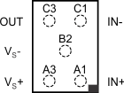
The OPA330 YFF package is a lead- (Pb-) free, die-level, wafer chip-scale package. Unlike devices that are in plastic packages, these devices have no molding compound, lead frame, wire bonds, or leads. Using standard surface-mount assembly procedures, the OPA330 YFF can be mounted to a printed-circuit board (PCB) without additional underfill. Figure 26 and Figure 27 detail the pinout and package marking, respectively. See the application note, NanoStar™ and NanoFree™ 300μm Solder Bump WCSP (SBVA017) for more detailed information on package characteristics and PCB design.
 Figure 26. DSBGA Pin Description
 Figure 27. YFF Package Marking
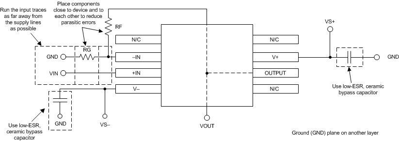
11.2 Layout Example
 Figure 28. OPAx330 Layout Example