SBOS492F June 2009 – May 2018 OPA2354A-Q1 , OPA354A-Q1 , OPA4354-Q1
PRODUCTION DATA.
- 1 Features
- 2 Applications
- 3 Description
- 4 Revision History
- 5 Pin Configuration and Functions
- 6 Specifications
- 7 Detailed Description
- 8 Application and Implementation
- 9 Power Supply Recommendations
- 10Layout
- 11Device and Documentation Support
- 12Mechanical, Packaging, and Orderable Information
Package Options
Mechanical Data (Package|Pins)
- PW|14
Thermal pad, mechanical data (Package|Pins)
Orderable Information
7.3.7 Capacitive Load and Stability
The OPAx354-Q1 family op amps can drive a wide range of capacitive loads. However, all op-amps under certain conditions can become unstable. Op amp configuration, gain, and load value are a few of the factors to consider when determining stability. An op amp in unity-gain configuration is most susceptible to the effects of capacitive loading. The capacitive load reacts with the output resistance of the op amp, along with any additional load resistance, to create a pole in the small-signal response that degrades the phase margin. For details, see Figure 15 (Frequency Response vs Capacitive Load.)
The OPAx354-Q1 topology enhances the ability of the device to drive capacitive loads. In unity gain, these op-amps perform well with large capacitive loads. For details see Figure 14, Recommended RS vs Capacitive Load, and Figure 15, Frequency Response vs Capacitive Load.
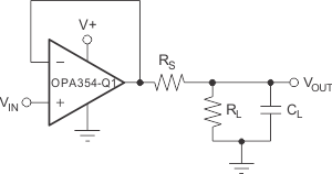
Insert a 10-Ω to 20-Ω resistor in series with the output to improve capacitive laod drive in the unity-gain configuration, as shown in Figure 35. This configuration significantly reduces ringing with large capacitive loads; see Figure 15 (Frequency Response vs Capacitive Load.) However, if a resistive load is in parallel with the capacitive load, RS creates a voltage divider. This configuration introduces a DC error at the output and slightly reduces output swing. This error may be insignificant. For example, if RL = 10 kΩ and RS = 20 Ω, the error at the output is approximately 0.2%.
 Figure 35. Series Resistor in Unity-Gain Configuration Improves Capacitive Load Drive