SBOS492F June   2009  – May 2018 OPA2354A-Q1 , OPA354A-Q1 , OPA4354-Q1

PRODUCTION DATA.  

  1. Features
  2. Applications
  3. Description
    1.     Simplified Schematic
  4. Revision History
  5. Pin Configuration and Functions
    1.     Pin Functions: OPA354A-Q1
    2.     Pin Functions: OPA2354A-Q1
    3.     Pin Functions: OPA4354-Q1
  6. Specifications
    1. 6.1 Absolute Maximum Ratings
    2. 6.2 ESD Ratings
    3. 6.3 Recommended Operating Conditions
    4. 6.4 Thermal Information: OPA354A-Q1
    5. 6.5 Thermal Information: OPA2354A-Q1
    6. 6.6 Thermal Information: OPA4354A-Q1
    7. 6.7 Electrical Characteristics
    8. 6.8 Typical Characteristics
  7. Detailed Description
    1. 7.1 Overview
    2. 7.2 Functional Block Diagram
    3. 7.3 Feature Description
      1. 7.3.1 Operating Voltage
      2. 7.3.2 Rail-to-Rail Input
      3. 7.3.3 Rail-to-Rail Output
      4. 7.3.4 Output Drive
      5. 7.3.5 Video
      6. 7.3.6 Driving Analog-to-Digital Converters
      7. 7.3.7 Capacitive Load and Stability
      8. 7.3.8 Wideband Transimpedance Amplifier
    4. 7.4 Device Functional Modes
  8. Application and Implementation
    1. 8.1 Application Information
    2. 8.2 Typical Applications
      1. 8.2.1 Transimpedance Amplifier
        1. 8.2.1.1 Design Requirements
        2. 8.2.1.2 Detailed Design Procedure
          1. 8.2.1.2.1 Optimizing The Transimpedance Circuit
        3. 8.2.1.3 Application Curve
      2. 8.2.2 High-Impedance Sensor Interface
      3. 8.2.3 Driving ADCs
      4. 8.2.4 Active Filter
  9. Power Supply Recommendations
    1. 9.1 Power Dissipation
  10. 10Layout
    1. 10.1 Layout Guidelines
    2. 10.2 Layout Example
  11. 11Device and Documentation Support
    1. 11.1 Documentation Support
      1. 11.1.1 Related Documentation
    2. 11.2 Related Links
    3. 11.3 Receiving Notification of Documentation Updates
    4. 11.4 Community Resources
    5. 11.5 Trademarks
    6. 11.6 Electrostatic Discharge Caution
    7. 11.7 Glossary
  12. 12Mechanical, Packaging, and Orderable Information

Package Options

Mechanical Data (Package|Pins)
Thermal pad, mechanical data (Package|Pins)
Orderable Information

Video

The OPAx354-Q1 output stage is capable of driving standard back-terminated 75-Ω video cables (see Figure 32). A back-terminated transmission line does not exhibit a capacitive load to the driver. A properly back-terminated 75-Ω cable does not appear as capacitance; the cable presents a 150-Ω resistive load to the OPAx354-Q1 output.
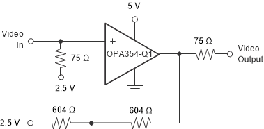
OPA354A-Q1 OPA2354A-Q1 OPA4354-Q1 ai_singl_sup_video_bos492.gifFigure 32. Single-Supply Video Line Driver

This series of amplifiers can be used as an amplifier for RGB graphic signals, which have a voltage of zero at the video black level by offsetting and AC-coupling the signal (see Figure 33).
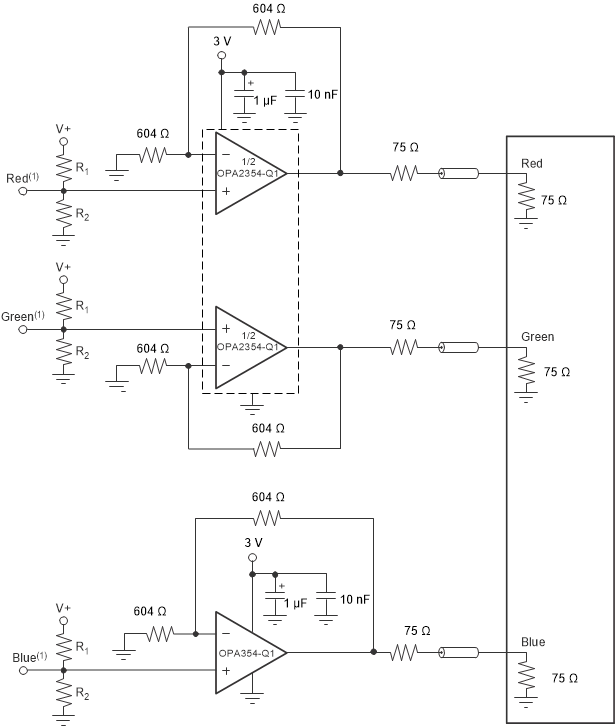
OPA354A-Q1 OPA2354A-Q1 OPA4354-Q1 ai_rgb_cable_drvr_bos492.gif
Source video signal offset 300 mV above ground to accommodate op amp swing to ground capability.
Figure 33. RGB Cable Driver