SBOS279F September 2003 – September 2016 OPA2373 , OPA2374 , OPA373 , OPA374 , OPA4374
PRODUCTION DATA.
- 1 Features
- 2 Applications
- 3 Description
- 4 Revision History
- 5 Device Comparison Table
- 6 Pin Configuration and Functions
-
7 Specifications
- 7.1 Absolute Maximum Ratings
- 7.2 ESD Ratings
- 7.3 Recommended Operating Conditions
- 7.4 Thermal Information: OPA373
- 7.5 Thermal Information: OPA374
- 7.6 Thermal Information: OPA2373
- 7.7 Thermal Information: OPA2374
- 7.8 Thermal Information: OPA4374
- 7.9 Electrical Characteristics: VS = 2.7 V to 5.5 V
- 7.10 Typical Characteristics
- 8 Detailed Description
- 9 Application and Implementation
- 10Power Supply Recommendations
- 11Layout
- 12Device and Documentation Support
- 13Mechanical, Packaging, and Orderable Information
Package Options
Mechanical Data (Package|Pins)
Thermal pad, mechanical data (Package|Pins)
Orderable Information
7 Specifications
7.1 Absolute Maximum Ratings
over operating free-air temperature range (unless otherwise noted)(1)| MIN | MAX | UNIT | ||
|---|---|---|---|---|
| Voltage | Supply | 7 | V | |
| Signal input pin(2) | −0.5 | (V+) + 0.5 | ||
| Current | Signal input pin(2) | –10 | 10 | mA |
| Output short-circuit(3) | Continuous | |||
| Temperature | Operating, TA | –55 | 150 | °C |
| Junction, TJ | 150 | |||
| Storage, Tstg | –65 | 150 | ||
(1) Stresses beyond those listed under Absolute Maximum Ratings may cause permanent damage to the device. These are stress ratings only, which do not imply functional operation of the device at these or any other conditions beyond those indicated under Recommended Operating Conditions. Exposure to absolute-maximum-rated conditions for extended periods may affect device reliability.
(2) Input terminals are diode-clamped to the power-supply rails. Input signals that can swing more than 0.5 V beyond the supply rails must be current limited to 10 mA or less.
(3) Short-circuit to ground, one amplifier per package.
7.2 ESD Ratings
| VALUE | UNIT | |||
|---|---|---|---|---|
| V(ESD) | Electrostatic discharge | Human-body model (HBM), per ANSI/ESDA/JEDEC JS-001(1) | ±3000 | V |
| Charged-device model (CDM), per JEDEC specification JESD22-C101(2) | ±1000 | |||
(1) JEDEC document JEP155 states that 500-V HBM allows safe manufacturing with a standard ESD control process.
(2) JEDEC document JEP157 states that 250-V CDM allows safe manufacturing with a standard ESD control process.
7.3 Recommended Operating Conditions
over operating free-air temperature range (unless otherwise noted)| MIN | MAX | UNIT | ||
|---|---|---|---|---|
| Supply voltage | ±1.35 (2.7) | ±2.75 (5.5) | V | |
| TA | Operating temperature | –40 | 125 | °C |
7.4 Thermal Information: OPA373
| THERMAL METRIC(1) | OPA373 | UNIT | ||
|---|---|---|---|---|
| D (SOIC) | DBV (SOT-23) | |||
| 8 PINS | 6 PINS | |||
| RθJA | Junction-to-ambient thermal resistance | 128.4 | 184.3 | °C/W |
| RθJC(top) | Junction-to-case (top) thermal resistance | 76.7 | 146.2 | °C/W |
| RθJB | Junction-to-board thermal resistance | 68.8 | 36.4 | °C/W |
| ψJT | Junction-to-top characterization parameter | 27.9 | 33.6 | °C/W |
| ψJB | Junction-to-board characterization parameter | 68.3 | 35.9 | °C/W |
| RθJC(bot) | Junction-to-case (bottom) thermal resistance | — | — | °C/W |
(1) For more information about traditional and new thermal metrics, see the Semiconductor and IC Package Thermal Metrics application report.
7.5 Thermal Information: OPA374
| THERMAL METRIC(1) | OPA374 | UNIT | ||
|---|---|---|---|---|
| D (SOIC) | DBV (SOT-23) | |||
| 8 PINS | 5 PINS | |||
| RθJA | Junction-to-ambient thermal resistance | 125.1 | 220.1 | °C/W |
| RθJC(top) | Junction-to-case (top) thermal resistance | 71.7 | 129 | °C/W |
| RθJB | Junction-to-board thermal resistance | 65.5 | 46.4 | °C/W |
| ψJT | Junction-to-top characterization parameter | 26.2 | 21 | °C/W |
| ψJB | Junction-to-board characterization parameter | 65 | 45.4 | °C/W |
| RθJC(bot) | Junction-to-case (bottom) thermal resistance | — | — | °C/W |
(1) For more information about traditional and new thermal metrics, see the Semiconductor and IC Package Thermal Metrics application report.
7.6 Thermal Information: OPA2373
| THERMAL METRIC(1) | OPA2373 | UNIT | ||
|---|---|---|---|---|
| DGS (VSON) | DRC (VSSOP) | |||
| 10 PINS | 10 PINS | |||
| RθJA | Junction-to-ambient thermal resistance | 170.6 | 56.4 | °C/W |
| RθJC(top) | Junction-to-case (top) thermal resistance | 59.8 | 76.7 | °C/W |
| RθJB | Junction-to-board thermal resistance | 91 | 30.6 | °C/W |
| ψJT | Junction-to-top characterization parameter | 10.4 | 3.7 | °C/W |
| ψJB | Junction-to-board characterization parameter | 89.6 | 30.7 | °C/W |
| RθJC(bot) | Junction-to-case (bottom) thermal resistance | — | 11.4 | °C/W |
(1) For more information about traditional and new thermal metrics, see the Semiconductor and IC Package Thermal Metrics application report.
7.7 Thermal Information: OPA2374
| THERMAL METRIC(1) | OPA2374 | UNIT | ||
|---|---|---|---|---|
| D (SOIC) | DCN (SOT-23) | |||
| 8 PINS | 8 PINS | |||
| RθJA | Junction-to-ambient thermal resistance | 117.8 | 171.3 | °C/W |
| RθJC(top) | Junction-to-case (top) thermal resistance | 63.1 | 73.5 | °C/W |
| RθJB | Junction-to-board thermal resistance | 58.4 | 106.3 | °C/W |
| ψJT | Junction-to-top characterization parameter | 19.3 | 15.4 | °C/W |
| ψJB | Junction-to-board characterization parameter | 57.9 | 105.5 | °C/W |
| RθJC(bot) | Junction-to-case (bottom) thermal resistance | — | — | °C/W |
(1) For more information about traditional and new thermal metrics, see the Semiconductor and IC Package Thermal Metrics application report.
7.8 Thermal Information: OPA4374
| THERMAL METRIC(1) | OPA4374 | UNIT | ||
|---|---|---|---|---|
| D (SOIC) | PW (TSSOP) | |||
| 14 PINS | 14 PINS | |||
| RθJA | Junction-to-ambient thermal resistance | 86.5 | 112.7 | °C/W |
| RθJC(top) | Junction-to-case (top) thermal resistance | 45 | 34.1 | °C/W |
| RθJB | Junction-to-board thermal resistance | 41.1 | 57.1 | °C/W |
| ψJT | Junction-to-top characterization parameter | 12.3 | 2.9 | °C/W |
| ψJB | Junction-to-board characterization parameter | 40.8 | 56.1 | °C/W |
| RθJC(bot) | Junction-to-case (bottom) thermal resistance | — | — | °C/W |
(1) For more information about traditional and new thermal metrics, see the Semiconductor and IC Package Thermal Metrics application report.
7.9 Electrical Characteristics: VS = 2.7 V to 5.5 V
At TA = 25°C, RL = 10 kΩ connected to VS/2, and VOUT = VS/2 (unless otherwise noted)| PARAMETER | TEST CONDITIONS | MIN | TYP | MAX | UNIT | ||
|---|---|---|---|---|---|---|---|
| OFFSET VOLTAGE | |||||||
| VOS | Input offset voltage | VS = 5 V | 1 | 5 | mV | ||
| Input offset voltage versus temperature |
TA = –40°C to 125°C | 6.5 | mV | ||||
| dVOS/dT | Input offset voltage versus drift |
TA = –40°C to +125°C | 3 | µV/°C | |||
| PSRR | Input offset voltage versus power supply |
VS = 2.7 V to 5.5 V, VCM < (V+) – 2 V |
TA = 25°C | 25 | 100 | µV/V | |
| TA = –40°C to 125°C | 150 | ||||||
| Channel separation, DC | 0.4 | µV/V | |||||
| At f = 1 kHz | 128 | dB | |||||
| INPUT VOLTAGE | |||||||
| VCM | Common-mode voltage range | (V–) – 0.2 | (V+) + 0.2 | V | |||
| CMRR | Common-mode rejection ratio | (V–) – 0.2 V < VCM < (V+) – 2 V | TA = 25°C | 80 | 90 | dB | |
| TA = –40°C to 125°C | 70 | ||||||
| VS = 5.5 V, (V–) – 0.2 V < VCM < (V+) + 0.2 V |
TA = 25°C | 66 | dB | ||||
| TA = –40°C to 125°C | 60 | dB | |||||
| INPUT BIAS CURRENT | |||||||
| IB | Input bias current | ±0.5 | ±10 | pA | |||
| IOS | Input offset current | ±0.5 | ±10 | pA | |||
| INPUT IMPEDANCE | |||||||
| Differential | 1013 || 3 | Ω || pF | |||||
| Common-mode | 1013 || 6 | Ω || pF | |||||
| NOISE | |||||||
| Input voltage noise | VCM < (V+) – 2 V, f = 0.1 Hz to 10 Hz | 10 | µVPP | ||||
| en | Input voltage noise density | VCM < (V+) – 2 V, f = 10 kHz | 15 | nV/√Hz | |||
| in | Input current noise density | VCM < (V+) – 2 V, f = 10 kHz | 4 | fA/√Hz | |||
| OPEN-LOOP GAIN | |||||||
| AOL | Open-loop voltage gain | VS = 5 V, RL = 100 kΩ, 0.025 V < VO < 4.975 V |
TA = 25°C | 94 | 110 | dB | |
| TA = –40°C to 125°C | 80 | ||||||
| VS = 5 V, RL = 5 kΩ, 0.125 V < VO < 4.875 V |
TA = 25°C | 94 | 106 | dB | |||
| TA = –40°C to 125°C | 80 | ||||||
| OUTPUT | |||||||
| Voltage output swing from rail | RL = 100 kΩ | TA = 25°C | 18 | 25 | mV | ||
| TA = –40°C to 125°C | 25 | mV | |||||
| RL = 5 kΩ | TA = 25°C | 100 | 125 | mV | |||
| TA = –40°C to 125°C | 125 | mV | |||||
| ISC | Short-circuit current | See Typical Characteristics | |||||
| CLOAD | Capacitive load drive | See Typical Characteristics | |||||
| RO | Open-loop output impedance | f = 1 MHz, IO = 0 mA | 220 | Ω | |||
| FREQUENCY RESPONSE | |||||||
| GBW | Gain-bandwidth product | CL = 100 pF | 6.5 | MHz | |||
| SR | Slew rate | CL = 100 pF, G = +1 | 5 | V/µs | |||
| tS | Settling time | 0.1%, CL = 100 pF, VS = 5 V, 2-V step, G = +1 |
1 | µs | |||
| 0.01%, CL = 100 pF, VS = 5 V, 2-V step, G = +1 |
1.5 | µs | |||||
| Overload recovery time | CL = 100 pF, VIN ● Gain > VS | 0.3 | µs | ||||
| THD+N | Total harmonic distortion + noise | CL = 100 pF, VS = 5 V, VO = 3 VPP, G = +1, f = 1 kHz |
0.0013% | ||||
| ENABLE OR SHUTDOWN | |||||||
| tOFF | Turnoff time | 3 | µs | ||||
| tON | Turnon time | 12 | µs | ||||
| VL | Logic low threshold | Shutdown | V– | (V–) + 0.8 | V | ||
| VH | Logic high threshold | Amplifier is active | (V–) + 2 | V+ | V | ||
| Input bias current of Enable pin | 0.2 | µA | |||||
| IQ(sd) | Quiescent current at shutdown (per amplifier) |
< 0.5 | 1 | µA | |||
| POWER SUPPLY | |||||||
| VS | Specified voltage range | 2.7 | 5.5 | V | |||
| Operating voltage range | 2.3 to 5.5 | V | |||||
| IQ | Quiescent current (per amplifier) |
IO = 0 mA | TA = 25°C | 585 | 750 | µA | |
| TA = –40°C to 125°C | 800 | µA | |||||
| TEMPERATURE | |||||||
| Specified range | –40 | 125 | °C | ||||
| TA | Operating range | –55 | 150 | °C | |||
| Tstg | Storage range | –65 | 150 | °C | |||
7.10 Typical Characteristics
At TA = 25°C, RL = 10 kΩ connected to VS/2, and VOUT = VS/2 (unless otherwise noted)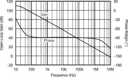 Figure 1. Open-Loop Gain and Phase vs Frequency
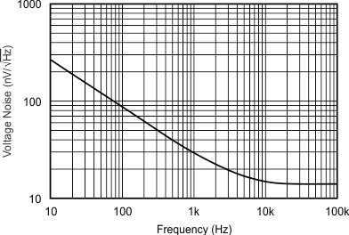 Figure 3. Input Voltage Noise Spectral Density vs Frequency
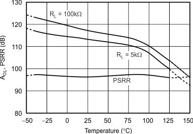 Figure 5. Open-Loop Gain and Power-Supply
Rejection Ratio vs Temperature
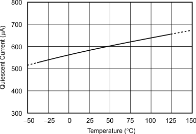 Figure 7. Quiescent Current vs Temperature
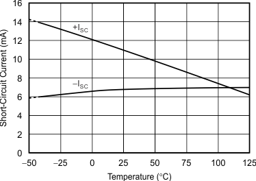 Figure 9. Short-Circuit Current vs Temperature
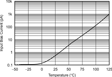 Figure 11. Input Bias Current vs Temperature
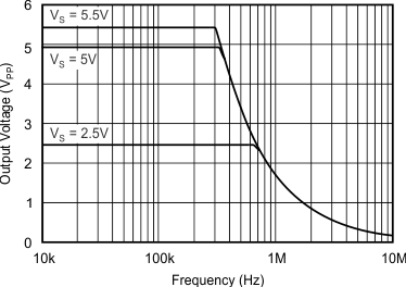 Figure 13. Maximum Output Voltage vs Frequency
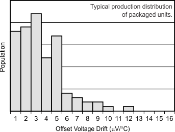 Figure 15. Offset Voltage Drift Magnitude
Production Distribution
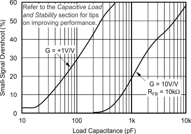 Figure 17. Small-Signal Overshoot vs Load Capacitance
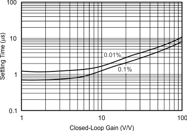 Figure 19. Settling Time vs Closed-Loop Gain
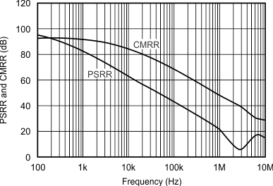 Figure 2. Power-Supply and Common-Mode
Rejection Ratio vs Frequency
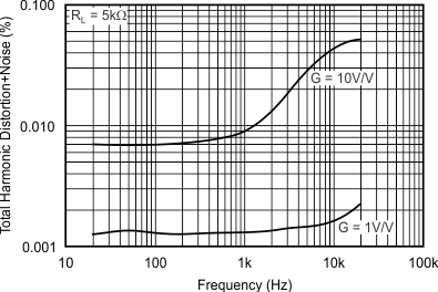 Figure 4. Total Harmonic Distortion + Noise vs Frequency
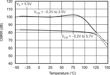 Figure 6. Common-Mode Rejection Ratio vs Temperature
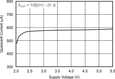 Figure 8. Quiescent Current vs Supply Voltage
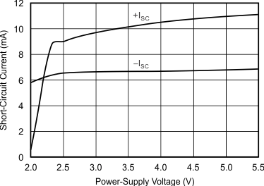 Figure 10. Continuous Short-Circuit Current
vs Power-Supply Voltage
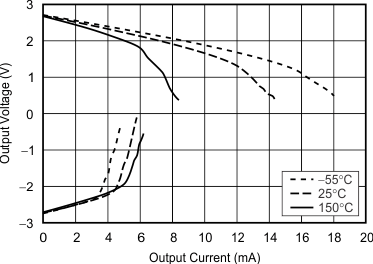 Figure 12. Output Voltage Swing vs Output Current
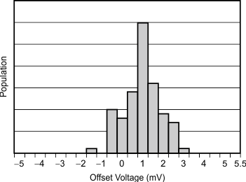 Figure 14. Offset Voltage Production Distribution
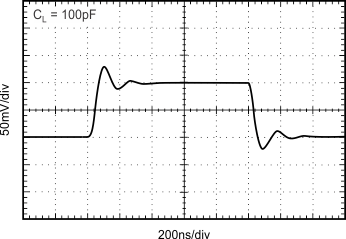 Figure 16. Small-Signal Step Response
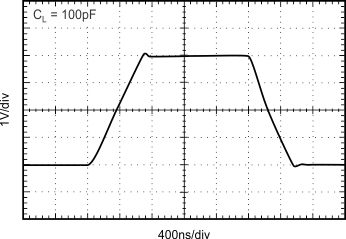 Figure 18. Large-Signal Step Response
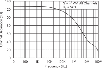 Figure 20. Channel Separation vs Frequency