SBOSA16 October 2020 OPA455
PRODUCTION DATA
- 1 Features
- 2 Applications
- 3 Description
- 4 Revision History
- 5 Pin Configuration and Functions
- 6 Specifications
- 7 Detailed Description
- 8 Application and Implementation
- 9 Power Supply Recommendations
- 10Layout
- 11Device and Documentation Support
- 12Mechanical, Packaging, and Orderable Information
Package Options
Mechanical Data (Package|Pins)
- DDA|8
Thermal pad, mechanical data (Package|Pins)
- DDA|8
Orderable Information
3 Description
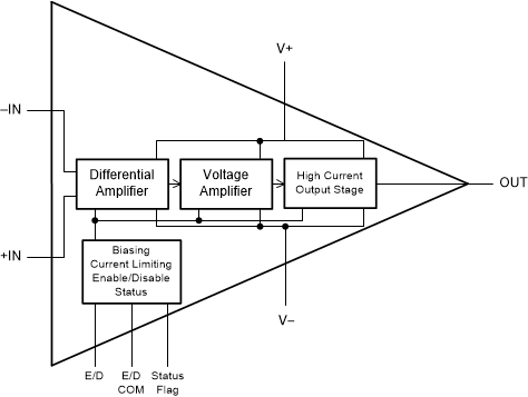
The OPA455 is a high-voltage (150-V), high current drive (45-mA), unity-gain stable operational amplifier with a gain-bandwidth product of 6.5 MHz and slew rate of 32 V/us. As a result of the amplifier wide output range, this device is an excellent choice for high-voltage piezo driving, avalance photodiode biasing, and high-voltage Howland current pump or voltage output stages.
The OPA455 is internally protected against overtemperature conditions and current overloads. The device is fully specified to perform over a wide power-supply range of ±6 V to ±75 V, or on a single supply of 12 V to 150 V. The status flag is an open-drain output that allows the device to be easily referenced to standard, low-voltage, logic circuitry. This high-voltage operational amplifier provides excellent accuracy and wide output swing, and is free from phase-inversion problems that are often found in similar amplifiers.
The output can be disabled using the enable-disable (E/D) pin. The E/D pin has a common return pin to allow for easy interface to low-voltage logic circuitry. This disable is accomplished without disturbing the input signal path, not only saving power but also protecting the load.
| PART NUMBER | PACKAGE(1) | BODY SIZE (NOM) |
|---|---|---|
| OPA455 | HSOIC (8) | 4.89 mm × 3.90 mm |
 OPA455 Block
Diagram
 Maximum Output
Voltage vs Frequency