SBOS933I February 2019 – August 2021 OPA2990 , OPA4990 , OPA990
PRODUCTION DATA
- 1 Features
- 2 Applications
- 3 Description
- 4 Revision History
- 5 Pin Configuration and Functions
- 6 Specifications
-
7 Detailed Description
- 7.1 Overview
- 7.2 Functional Block Diagram
- 7.3
Feature Description
- 7.3.1 Input Protection Circuitry
- 7.3.2 EMI Rejection
- 7.3.3 Thermal Protection
- 7.3.4 Capacitive Load and Stability
- 7.3.5 Common-Mode Voltage Range
- 7.3.6 Phase Reversal Protection
- 7.3.7 Electrical Overstress
- 7.3.8 Overload Recovery
- 7.3.9 Typical Specifications and Distributions
- 7.3.10 Packages With an Exposed Thermal Pad
- 7.3.11 Shutdown
- 7.4 Device Functional Modes
- 8 Application and Implementation
- 9 Power Supply Recommendations
- 10Layout
- 11Device and Documentation Support
- 12Mechanical, Packaging, and Orderable Information
Package Options
Mechanical Data (Package|Pins)
Thermal pad, mechanical data (Package|Pins)
Orderable Information
8.2.1 High Voltage Buffered Multiplexer
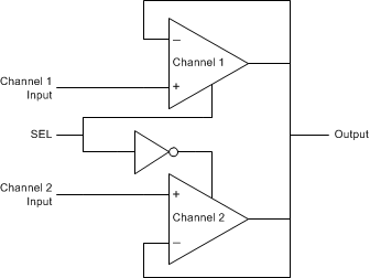
The OPAx990S shutdown devices can be configured to create a high voltage, buffered multiplexer. Outputs can be connected together on a common bus and the shutdown pins can be used to select the desired channel to pass through. Since the amplifier circuitry has been designed such that disable transitions occur significantly faster than enable transitions, the amplifier naturally exhibits a "break before make" switch topology. Amplifier outputs enter a high impedance state when placed in shutdown, so there is no risk of bus contention when connecting multiple channel outputs together. Additionally, because outputs are isolated from inputs, there is no concern about the impedance at the input of each channel interacting undesirably with the impedance at the output, like an amplifier gain stage or ADC driver circuit. Also, because this topology uses amplifiers instead of MOSFET switches, other common issues with multiplexers such as charge injection or signal error due to RON effects are eliminated.
Figure 8-1 shows an example topology for a basic 2:1 multiplexer. When SEL is low, channel 1 is selected and active; when SEL is high, channel 2 is selected and active. For more information on how to use the OPAx990S shutdown function, see the shutdown section in the Electrical Characteristics table.
 Figure 8-1 High Voltage Buffered Multiplexer