SBOS969F October 2019 – January 2022 OPA2991 , OPA4991 , OPA991
PRODMIX
- 1 Features
- 2 Applications
- 3 Description
- 4 Revision History
- 5 Pin Configuration and Functions
- 6 Specifications
-
7 Detailed Description
- 7.1 Overview
- 7.2 Functional Block Diagram
- 7.3
Feature Description
- 7.3.1 Input Protection Circuitry
- 7.3.2 EMI Rejection
- 7.3.3 Thermal Protection
- 22
- 7.3.4 Capacitive Load and Stability
- 7.3.5 Common-Mode Voltage Range
- 7.3.6 Phase Reversal Protection
- 7.3.7 Electrical Overstress
- 7.3.8 Overload Recovery
- 7.3.9 Typical Specifications and Distributions
- 7.3.10 Packages With an Exposed Thermal Pad
- 7.3.11 Shutdown
- 7.4 Device Functional Modes
- 8 Application and Implementation
- 9 Power Supply Recommendations
- 10Layout
- 11Device and Documentation Support
- 12Mechanical, Packaging, and Orderable Information
Package Options
Mechanical Data (Package|Pins)
Thermal pad, mechanical data (Package|Pins)
- PW|14
Orderable Information
5 Pin Configuration and Functions
DRL package is preview
only.
Figure 5-1 OPA991 DBV, T DCK, and
DRL Package(A)5-Pin SOT-23, SC70, and SOT-553
(Top View)
Figure 5-2 OPA991 DCK
Package
5-Pin SC70
(Top View)
5-Pin SC70
(Top View)
Table 5-1 Pin Functions: OPA991
| PIN | I/O | DESCRIPTION | ||
|---|---|---|---|---|
| NAME | DBV, DRL | DCK | ||
| IN+ | 3 | 1 | I | Noninverting input |
| IN– | 4 | 3 | I | Inverting input |
| OUT | 1 | 4 | O | Output |
| V+ | 5 | 5 | — | Positive (highest) power supply |
| V– | 2 | 2 | — | Negative (lowest) power supply |

DRL package is preview
only.
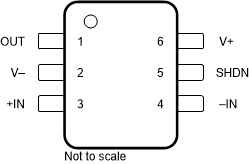
Figure 5-3 OPA991S DBV and DRL Package(A)6-Pin SOT-23 and SOT-563
(Top View)
Table 5-2 Pin Functions: OPA991S
| PIN | I/O | DESCRIPTION | |
|---|---|---|---|
| NAME | NO. | ||
| +IN | 3 | I | Noninverting input |
| –IN | 4 | I | Inverting input |
| OUT | 1 | O | Output |
| SHDN | 5 | I | Shutdown: low = amplifier enabled, high = amplifier disabled. See Section 7.3.11 for more information. |
| V+ | 6 | — | Positive (highest) power supply |
| V– | 2 | — | Negative (lowest) power supply |
Figure 5-4 OPA2991 D, DDF, DGK, and PW Package
8-Pin SOIC, SOT-23, TSSOP, and VSSOP
(Top View)
8-Pin SOIC, SOT-23, TSSOP, and VSSOP
(Top View)
Connect thermal pad to V–.
See Section 7.3.10 for more information.
Figure 5-5 OPA2991 DSG Package(A)8-Pin WSON With Exposed Thermal Pad
(Top View)
Table 5-3 Pin Functions: OPA2991
| PIN | I/O | DESCRIPTION | |
|---|---|---|---|
| NAME | NO. | ||
| +IN A | 3 | I | Noninverting input, channel A |
| +IN B | 5 | I | Noninverting input, channel B |
| –IN A | 2 | I | Inverting input, channel A |
| –IN B | 6 | I | Inverting input, channel B |
| OUT A | 1 | O | Output, channel A |
| OUT B | 7 | O | Output, channel B |
| V+ | 8 | — | Positive (highest) power supply |
| V– | 4 | — | Negative (lowest) power supply |

Package is preview
only.
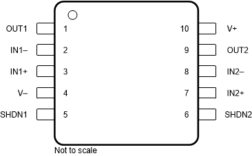
Figure 5-6 OPA2991S DGS Package(A)10-Pin VSSOP
(Top View)
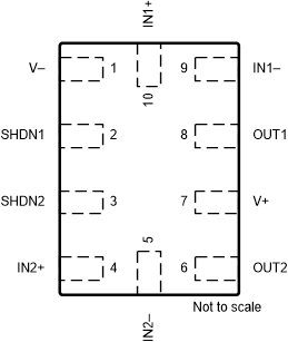
 Figure 5-7 OPA2991S RUG Package
10-Pin X2QFN
(Top View)
Table 5-4 Pin Functions: OPA2991S
| PIN | I/O | DESCRIPTION | ||
|---|---|---|---|---|
| NAME | VSSOP | X2QFN | ||
| +IN A | 3 | 10 | I | Noninverting input, channel A |
| +IN B | 7 | 4 | I | Noninverting input, channel B |
| –IN A | 2 | 9 | I | Inverting input, channel A |
| –IN B | 8 | 5 | I | Inverting input, channel B |
| OUT A | 1 | 8 | O | Output, channel A |
| OUT B | 9 | 6 | O | Output, channel B |
| SHDN1 | 5 | 2 | I | Shutdown, channel 1: low = amplifier enabled, high = amplifier disabled. See Section 7.3.11 for more information. |
| SHDN2 | 6 | 3 | I | Shutdown, channel 2: low = amplifier enabled, high = amplifier disabled. See Section 7.3.11 for more information. |
| V+ | 10 | 7 | — | Positive (highest) power supply |
| V– | 4 | 1 | — | Negative (lowest) power supply |
Figure 5-8 OPA4991 D, PW, and DYY Packages
14-Pin SOIC, TSSOP, SOT-23
(Top View)
14-Pin SOIC, TSSOP, SOT-23
(Top View)
Figure 5-9 OPA4991 RUC Package
14-Pin X2QFN
(Top View)
14-Pin X2QFN
(Top View)
Table 5-5 Pin Functions: OPA4991
| PIN | I/O | DESCRIPTION | ||
|---|---|---|---|---|
| NAME | SOIC, TSSOP, SOT-23 | X2QFN | ||
| IN1+ | 3 | 2 | I | Noninverting input, channel 1 |
| IN1– | 2 | 1 | I | Inverting input, channel 1 |
| IN2+ | 5 | 4 | I | Noninverting input, channel 2 |
| IN2– | 6 | 5 | I | Inverting input, channel 2 |
| IN3+ | 10 | 9 | I | Noninverting input, channel 3 |
| IN3– | 9 | 8 | I | Inverting input, channel 3 |
| IN4+ | 12 | 11 | I | Noninverting input, channel 4 |
| IN4– | 13 | 12 | I | Inverting input, channel 4 |
| NC | — | — | — | Do not connect |
| OUT1 | 1 | 14 | O | Output, channel 1 |
| OUT2 | 7 | 6 | O | Output, channel 2 |
| OUT3 | 8 | 7 | O | Output, channel 3 |
| OUT4 | 14 | 13 | O | Output, channel 4 |
| V+ | 4 | 3 | — | Positive (highest) power supply |
| V– | 11 | 10 | — | Negative (lowest) power supply |