SBOS070D October   1997  – December 2019 OPA548

PRODUCTION DATA.  

  1. Features
  2. Applications
    1.     Simplified Schematic
  3. Description
  4. Revision History
  5. Pin Configuration and Functions
    1.     Pin Functions
  6. Specifications
    1. 6.1 Absolute Maximum Ratings
    2. 6.2 ESD Ratings
    3. 6.3 Recommended Operating Conditions
    4. 6.4 Thermal Information
    5. 6.5 Electrical Characteristics
    6. 6.6 Typical Characteristics
  7. Detailed Description
    1. 7.1 Overview
    2. 7.2 Functional Block Diagram
    3. 7.3 Feature Description
      1. 7.3.1 Adjustable Current Limit
      2. 7.3.2 Enable/Status (E/S) Pin
      3. 7.3.3 Thermal Shutdown Status
    4. 7.4 Device Functional Modes
      1. 7.4.1 Output Disable
  8. Application and Implementation
    1. 8.1 Application Information
    2. 8.2 Typical Applications
      1. 8.2.1 Basic Circuit Connections
        1. 8.2.1.1 Design Requirements
        2. 8.2.1.2 Detailed Design Procedure
          1. 8.2.1.2.1 Power Supply Requirements
          2. 8.2.1.2.2 Gain Setting and Input Configuration
          3. 8.2.1.2.3 Current Limit
          4. 8.2.1.2.4 Safe-Operating-Area
          5. 8.2.1.2.5 Heat Sinking
        3. 8.2.1.3 Application Curve
      2. 8.2.2 Monitoring Single- and Dual-Supplies
        1. 8.2.2.1 Design Requirements
        2. 8.2.2.2 Detailed Design Procedure
          1. 8.2.2.2.1 Output Disable and Thermal Shutdown Status
      3. 8.2.3 Programmable Power Supply
    3. 8.3 System Examples
  9. Power Supply Recommendations
    1. 9.1 Output Stage Compensation
    2. 9.2 Output Protection
  10. 10Layout
    1. 10.1 Layout Guidelines
      1. 10.1.1 Safe Operating Area
      2. 10.1.2 Amplifier Mounting
      3. 10.1.3 Power Dissipation
      4. 10.1.4 Thermal Considerations
      5. 10.1.5 Heat Sinking
        1. 10.1.5.1 Heat Sink Selection Example
    2. 10.2 Layout Example
  11. 11Device and Documentation Support
    1. 11.1 Device Support
      1. 11.1.1 Third-Party Products Disclaimer
    2. 11.2 Documentation Support
      1. 11.2.1 Related Documentation
    3. 11.3 Receiving Notification of Documentation Updates
    4. 11.4 Support Resources
    5. 11.5 Trademarks
    6. 11.6 Electrostatic Discharge Caution
    7. 11.7 Glossary
  12. 12Mechanical, Packaging, and Orderable Information

Package Options

Mechanical Data (Package|Pins)
Thermal pad, mechanical data (Package|Pins)
Orderable Information

Output Disable

A unique feature of the OPA548 is its output disable capability. This function not only conserves power during idle periods (quiescent current drops to approximately 6 mA), but also allows multiplexing in low frequency (f < 20 kHz), multichannel applications. Signals greater than 20 kHz may cause leakage current to increase in devices that are shutdown. Figure 33 shows the two OPA548s in a switched amplifier configuration. The ON/OFF state of the two amplifiers is controlled by the voltage on the E/S pin.

To disable the output, the E/S pin is pulled LOW, no greater than 0.8 V more than the negative rail. Typically the output is shutdown in 1 μs. Figure 23 provides an example of how to implement this function using a single supply. Figure 24 gives a circuit for dual-supply applications. To return the output to an enabled state, the E/S pin should be disconnected (open) or pulled to at least (V–) + 2.4 V. It should be noted that pulling the E/S pin HIGH (output enabled) does not disable internal thermal shutdown.
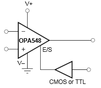
OPA548 outputdis1.pngFigure 23. Output Disable With a Single Supply
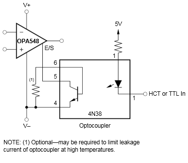
OPA548 outputdis2.pngFigure 24. Output Disable With Dual Supplies