SBOS196I December 2001 – February 2024 OPA656
PRODUCTION DATA
- 1
- 1 Features
- 2 Applications
- 3 Description
- 4 Device Comparison Table
- 5 Pin Configuration and Functions
- 6 Specifications
- 7 Detailed Description
- 8 Application and Implementation
- 9 Device and Documentation Support
- 10Revision History
- 11Mechanical, Packaging, and Orderable Information
Package Options
Refer to the PDF data sheet for device specific package drawings
Mechanical Data (Package|Pins)
- D|8
- DBV|5
Thermal pad, mechanical data (Package|Pins)
Orderable Information
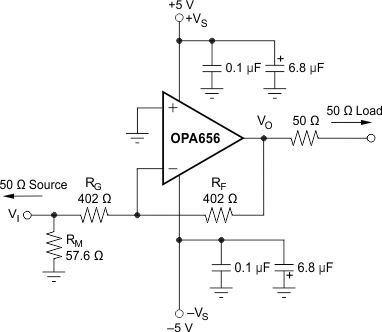
8.1.2 Wideband, Inverting Gain Operation
The circuit of Figure 8-2 shows the inverting gain of –1 V/V test circuit used for most of the inverting typical characteristics. In this case, an additional resistor RM is used to achieve the 50‑Ω input impedance required by the test equipment using in characterization. This input impedance matching is optional in a circuit board environment where the OPA656 is used as an inverting amplifier at the output of a prior stage.
In this configuration, the feedback resistor acts as an additional load at output in parallel with the 100-Ω load used for test. Increase the RF value to decrease the loading on the output (improving harmonic distortion) with the constraint that the parallel combination of RF || RG < 200 Ω. For higher gains with the dc precision provided by the FET input OPA656, consider the higher gain bandwidth product OPA814 or OPA818.
 Figure 8-2 Inverting G = –1 V/V Specifications and Test Circuit
Figure 8-2 also shows the noninverting input tied directly to ground. Often, a bias current canceling resistor to ground is included here to null out the dc errors caused by input bias current effects. This resistor is only useful when the input bias currents are matched. For a JFET part such as the OPA656, the input bias currents do not match but are so low to begin with (< 20 pA) that dc errors due to input bias currents are negligible. Thus, no resistor is recommended at the noninverting inputs for the inverting signal path condition.