SBOS673D September 2017 – December 2018 OPA2837 , OPA837
PRODUCTION DATA.
- 1 Features
- 2 Applications
- 3 Description
- 4 Revision History
- 5 Pin Configuration and Functions
-
6 Specifications
- 6.1 Absolute Maximum Ratings
- 6.2 ESD Ratings
- 6.3 Recommended Operating Conditions
- 6.4 Thermal Information: OPA837
- 6.5 Thermal Information: OPA2837
- 6.6 Electrical Characteristics: VS = 5 V
- 6.7 Electrical Characteristics: VS = 3 V
- 6.8 Typical Characteristics: VS = 5.0 V
- 6.9 Typical Characteristics: VS = 3.0 V
- 6.10 Typical Characteristics: ±2.5-V to ±1.5-V Split Supply
- 7 Detailed Description
-
8 Application and Implementation
- 8.1
Application Information
- 8.1.1 Noninverting Amplifier
- 8.1.2 Inverting Amplifier
- 8.1.3 Output DC Error Calculations
- 8.1.4 Output Noise Calculations
- 8.1.5 Instrumentation Amplifier
- 8.1.6 Attenuators
- 8.1.7 Differential to Single-Ended Amplifier
- 8.1.8 Differential-to-Differential Amplifier
- 8.1.9 Pulse Application With Single-Supply Circuit
- 8.1.10 ADC Driver Performance
- 8.2 Typical Applications
- 8.1
Application Information
- 9 Power Supply Recommendations
- 10Layout
- 11Device and Documentation Support
- 12Mechanical, Packaging, and Orderable Information
Package Options
Mechanical Data (Package|Pins)
Thermal pad, mechanical data (Package|Pins)
Orderable Information
8.2.1 Active Filters
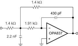
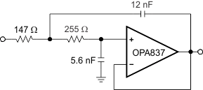
The OPAx837 is a good choice for active filters. Figure 83 and Figure 84 show MFB and Sallen-Key circuits designed implementing second-order, low-pass Butterworth filter circuits. Figure 85 illustrates the frequency response.
The main difference is that the MFB active filter provides an inverting amplifier in the pass band and the Sallen-Key active filter is noninverting. The primary advantage for each active filter is that the Sallen-Key filter in unity gain has no resistor gain error term or feedback resistor noise contribution. The MFB active filter has better attenuation properties beyond the bandwidth of the op amp. The example circuits are assuming a split-supply operation but single-supply operation is possible with midscale biasing.
 Figure 83. MFB Active Filter, 100-kHz, Second-Order, Low-Pass Butterworth Filter Circuit
  Figure 84. Sallen-Key Active Filter, 100-kHz, Second-Order, Low-Pass Butterworth Filter Circuit