SBOS673D September 2017 – December 2018 OPA2837 , OPA837
PRODUCTION DATA.
- 1 Features
- 2 Applications
- 3 Description
- 4 Revision History
- 5 Pin Configuration and Functions
-
6 Specifications
- 6.1 Absolute Maximum Ratings
- 6.2 ESD Ratings
- 6.3 Recommended Operating Conditions
- 6.4 Thermal Information: OPA837
- 6.5 Thermal Information: OPA2837
- 6.6 Electrical Characteristics: VS = 5 V
- 6.7 Electrical Characteristics: VS = 3 V
- 6.8 Typical Characteristics: VS = 5.0 V
- 6.9 Typical Characteristics: VS = 3.0 V
- 6.10 Typical Characteristics: ±2.5-V to ±1.5-V Split Supply
- 7 Detailed Description
-
8 Application and Implementation
- 8.1
Application Information
- 8.1.1 Noninverting Amplifier
- 8.1.2 Inverting Amplifier
- 8.1.3 Output DC Error Calculations
- 8.1.4 Output Noise Calculations
- 8.1.5 Instrumentation Amplifier
- 8.1.6 Attenuators
- 8.1.7 Differential to Single-Ended Amplifier
- 8.1.8 Differential-to-Differential Amplifier
- 8.1.9 Pulse Application With Single-Supply Circuit
- 8.1.10 ADC Driver Performance
- 8.2 Typical Applications
- 8.1
Application Information
- 9 Power Supply Recommendations
- 10Layout
- 11Device and Documentation Support
- 12Mechanical, Packaging, and Orderable Information
Package Options
Mechanical Data (Package|Pins)
Thermal pad, mechanical data (Package|Pins)
Orderable Information
8.1.2 Inverting Amplifier
The OPAx837 can be used as an inverting amplifier with a signal input to the inverting input, VIN–, through the gain-setting resistor RG. A basic block diagram of the circuit is illustrated in Figure 63.
The output of the amplifier can be calculated according to Equation 3 if VIN = VREF + VSIG and the noninverting input is biased to VREF.

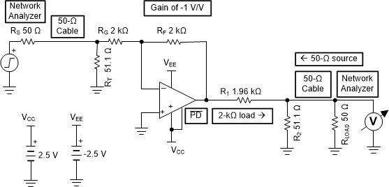
The signal gain of the circuit is set by Equation 4 and VREF provides a reference point around which the input and output signals swing. For bipolar-supply operation, VREF is often ground. The output signal is 180˚ out-of-phase with the input signal in the pass band of the application. Figure 75 shows the 50-Ω input matched configuration used for the inverting characterization plots set up for a gain of –1 V/V. In this case, an added termination resistor, RT, is placed in parallel with the input RG resistor to provide an impedance match to 50-Ω test equipment. The output network appears as a 2-kΩ load but with a 50-Ω source to the network analyzer. This output interface network does add a 37.9-dB insertion loss that is normalized out in the characterization curves. Table 3 lists the suggested values for RF, RG, and RT for inverting gains from –0.5 V/V to –10 V/V. If a 50-Ω input match is not required, eliminate the RT element.

Table 3. Inverting Recommended Resistor Values
| INVERTING GAIN (V/V) | RF (Ω) | RG (Ω) | STANDARD RT (Ω) | INPUT ZI (Ω) | ACTUAL (V/V) | GAIN (dB) |
|---|---|---|---|---|---|---|
| –0.5 | 1190 | 2370 | 51.1 | 50.02 | –0.50 | –5.98 |
| –1 | 2000 | 2000 | 51.1 | 49.83 | –1.00 | 0.00 |
| –2 | 2260 | 1130 | 52.3 | 49.99 | –2.00 | 6.02 |
| –3 | 2370 | 787 | 53.6 | 50.18 | –3.01 | 9.58 |
| –4 | 2490 | 619 | 54.9 | 50.43 | –4.02 | 12.09 |
| –5 | 2550 | 511 | 54.9 | 49.57 | –4.99 | 13.96 |
| –6 | 2610 | 432 | 56.2 | 49.73 | –6.04 | 15.62 |
| –7 | 2670 | 383 | 57.6 | 50.07 | –6.97 | 16.87 |
| –8 | 2670 | 332 | 59 | 50.10 | –8.04 | 18.11 |
| –9 | 2670 | 294 | 60.4 | 50.11 | –9.08 | 19.16 |
| –10 | 2670 | 267 | 61.9 | 50.25 | –10.00 | 20.00 |
