SBOS867C August   2017  – October 2023 OPA838

PRODUCTION DATA  

  1.   1
  2. Features
  3. Applications
  4. Description
  5. Revision History
  6. Device Comparison Table
  7. Pin Configuration and Functions
  8. Specifications
    1. 7.1 Absolute Maximum Ratings
    2. 7.2 ESD Ratings
    3. 7.3 Recommended Operating Conditions
    4. 7.4 Thermal Information
    5. 7.5 Electrical Characteristics: VS = 5 V
    6. 7.6 Electrical Characteristics: VS = 3 V
    7. 7.7 Typical Characteristics: VS = 5 V
    8. 7.8 Typical Characteristics: VS = 3 V
    9. 7.9 Typical Characteristics: Over Supply Range
  9. Detailed Description
    1. 8.1 Overview
    2. 8.2 Functional Block Diagram
    3. 8.3 Feature Description
      1. 8.3.1 Input Common-Mode Voltage Range
      2. 8.3.2 Output Voltage Range
      3. 8.3.3 Power-Down Operation
      4. 8.3.4 Trade-Offs in Selecting The Feedback Resistor Value
      5. 8.3.5 Driving Capacitive Loads
    4. 8.4 Device Functional Modes
      1. 8.4.1 Split-Supply Operation (±1.35 V to ±2.7 V)
      2. 8.4.2 Single-Supply Operation (2.7 V to 5.4 V)
      3. 8.4.3 Power Shutdown Operation
  10. Application and Implementation
    1. 9.1 Application Information
      1. 9.1.1 Noninverting Amplifier
      2. 9.1.2 Inverting Amplifier
      3. 9.1.3 Output DC Error Calculations
      4. 9.1.4 Output Noise Calculations
    2. 9.2 Typical Applications
      1. 9.2.1 High-Gain Differential I/O Designs
        1. 9.2.1.1 Design Requirements
        2. 9.2.1.2 Detailed Design Procedure
        3. 9.2.1.3 Application Curves
      2. 9.2.2 Transimpedance Amplifier
        1. 9.2.2.1 Design Requirements
        2. 9.2.2.2 Detailed Design Procedure
        3. 9.2.2.3 Application Curve
    3. 9.3 Power Supply Recommendations
    4. 9.4 Layout
      1. 9.4.1 Layout Guidelines
      2. 9.4.2 Layout Example
  11. 10Device and Documentation Support
    1. 10.1 Device Support
      1. 10.1.1 TINA-TI™ Simulation Model Features
    2. 10.2 Documentation Support
      1. 10.2.1 Related Documentation
    3. 10.3 Receiving Notification of Documentation Updates
    4. 10.4 Support Resources
    5. 10.5 Trademarks
    6. 10.6 Electrostatic Discharge Caution
    7. 10.7 Glossary
  12.   Mechanical, Packaging, and Orderable Information

Package Options

Mechanical Data (Package|Pins)
Thermal pad, mechanical data (Package|Pins)
Orderable Information

Typical Characteristics: VS = 5 V

at VS+ = 5 V, VS– = 0 V, RF = 1 kΩ, RG = 200 Ω, RL = 2 kΩ, G = 6 V/V, input and output referenced to midsupply, and TA ≈ 25°C (unless otherwise noted)
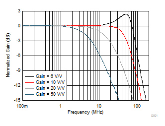
GUID-68783816-49D6-435F-B6BF-559DE7A281AA-low.gif
See Figure 9-1 and Table 9-1 (VO = 20 mVPP, R LOAD = 2 kΩ)
Figure 7-1 Noninverting Small-Signal Frequency Response vs Gain
GUID-63788CC5-1A60-4673-A406-FEF5A0CFA984-low.gif
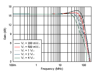
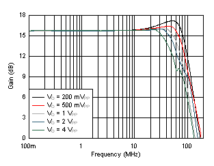
Gain = 6 V/V, R LOAD = 2 kΩ
Figure 7-3 Noninverting Large-Signal Bandwidth vs VOPP
GUID-5C01F120-481F-4A32-A3C7-F17224F575E9-low.gif
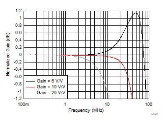
See Figure 9-1 and Table 9-1 (VO = 200 mVPP, R LOAD = 2 kΩ)
Figure 7-5 Noninverting Response Flatness vs Gain
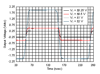
GUID-37A65B87-ECED-4EC1-AF32-B5CC60811601-low.gif
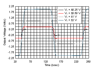
See Figure 9-1 (gain of 6 V/V)
Figure 7-7 Noninverting Step Response vs VOPP
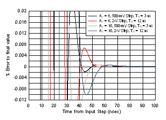
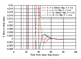
GUID-B38C03A5-95F3-40A2-9B5F-B0DE5C0A3696-low.gifFigure 7-9 Simulated Noninverting Settling Time
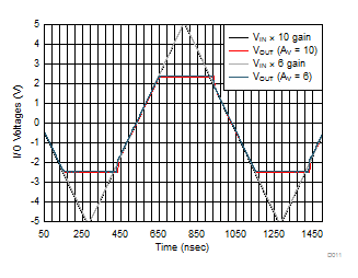
GUID-1E4F0100-9DE3-4ACD-A027-8272D997016E-low.gifFigure 7-11 Noninverting Overdrive Recovery
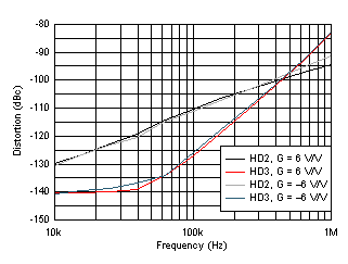
GUID-8429DF5E-9BFF-4F81-9FF8-F5F3AC2CD592-low.gifFigure 7-13 Harmonic Distortion vs Frequency
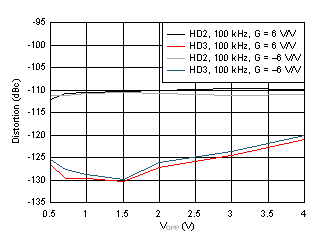
GUID-7EBA5DA1-7D35-458B-9B5A-8718E9E2FEFD-low.gif
See Figure 9-1, Figure 9-2, Table 9-1, and Table 9-2
f = 100 kHz, RLOAD = 2 kΩ
Figure 7-15 Harmonic Distortion vs Output Swing
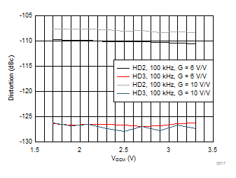
GUID-D3C5CD07-F16B-4A30-AAB6-504D438F4B6D-low.gif
See Figure 9-1 and Table 9-1
VO = 2 VPP, f = 100 kHz, RLOAD = 2 kΩ
Figure 7-17 Noninverting Distortion vs Output Common-Mode Voltage
GUID-2526D7AA-E4E7-4EE5-9767-1F54E2A5C103-low.gif
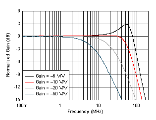
See Figure 9-2 and Table 9-2 (VO = 20 mVPP, R LOAD= 2 kΩ)
Figure 7-2 Inverting Small-Signal Frequency Response vs Gain
GUID-ED86F439-0520-469A-B87E-1A8ECF8856C5-low.gif
Gain = –6 V/V, R LOAD = 2 kΩ
Figure 7-4 Inverting Large-Signal Bandwidth vs VOPP
GUID-39ECDF38-87D9-4576-8BD0-44E61659EDC4-low.gif
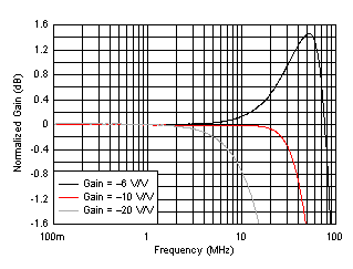
See Figure 9-2 and Table 9-2 (VO = 200 mVPP; R LOAD = 2 kΩ)
Figure 7-6 Inverting Response Flatness vs Gain
GUID-36D94EB1-B4B5-4346-8F38-BEFE58797A3D-low.gif
See Figure 9-2 (gain of –6 V/V)
Figure 7-8 Inverting Step Response vs VOPP
GUID-45263CAA-87E0-4F23-B48B-6335C8E0601B-low.gifFigure 7-10 Simulated Inverting Settling Time
GUID-62567EE2-F012-4379-838D-9A5718FDA90F-low.gifFigure 7-12 Inverting Overdrive Recovery
GUID-2BEFE833-73F2-4507-94C4-E8F55C5B72C1-low.gif
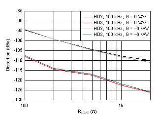
See Figure 9-1, Figure 9-2, Table 9-1, and Table 9-2
VO = 2 VPP, f = 100 kHz
Figure 7-14 Harmonic Distortion vs RLOAD
GUID-4D102004-6FFF-4F2C-8747-590A6DA02CDC-low.gif
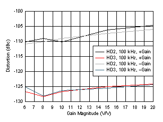
See Figure 9-1, Figure 9-2, Table 9-1, and Table 9-2
VO = 2 VPP, RLOAD = 2 kΩ, f = 100 kHz
Figure 7-16 Harmonic Distortion vs Gain
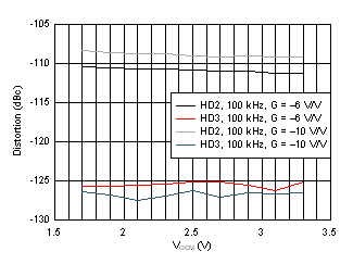
GUID-C47B0D2C-D094-4F99-B3BB-1CF2FD50661D-low.gif
See Figure 9-2 and Table 9-2
VO = 2 VPP, f = 100 kHz, RLOAD = 2 kΩ
Figure 7-18 Inverting Distortion vs Output Common-Mode Voltage