SBOSA10F June 2021 – March 2024 OPA2992 , OPA4992 , OPA992
PRODUCTION DATA
- 1
- 1 Features
- 2 Applications
- 3 Description
- 4 Pin Configuration and Functions
- 5 Specifications
-
6 Detailed Description
- 6.1 Overview
- 6.2 Functional Block Diagram
- 6.3
Feature Description
- 6.3.1 Input Protection Circuitry
- 6.3.2 EMI Rejection
- 6.3.3 Thermal Protection
- 6.3.4 Capacitive Load and Stability
- 6.3.5 Common-Mode Voltage Range
- 6.3.6 Phase Reversal Protection
- 6.3.7 Electrical Overstress
- 6.3.8 Overload Recovery
- 6.3.9 Typical Specifications and Distributions
- 6.3.10 Packages With an Exposed Thermal Pad
- 6.3.11 Shutdown
- 6.4 Device Functional Modes
- 7 Application and Implementation
- 8 Device and Documentation Support
- 9 Revision History
- 10Mechanical, Packaging, and Orderable Information
Package Options
Mechanical Data (Package|Pins)
Thermal pad, mechanical data (Package|Pins)
Orderable Information
3 Description
The OPAx992 family (OPA992, OPA2992, and OPA4992) is a family of high voltage (40V) general purpose operational amplifiers. These devices offer excellent DC precision and AC performance, including rail-to-rail input/output, low offset (±210µV, typical), low offset drift (±0.25µV/°C, typical) and low noise (7nV/√Hz at 1kHz, 4.4nV/√Hz at 10kHz).
Features such as differential and common-mode input voltage ranges to the supply rails, high short-circuit current (±65mA), and high slew rate (32V/µs) make the OPAx992 a flexible, robust, and high-performance op amp for high-voltage industrial applications.
The OPAx992 family of op amps is available in small-size packages (such as X2QFN and WSON), as well as standard packages (such as SOT-23, SOIC, and TSSOP), and is specified from –40°C to 125°C.
| PART NUMBER(1) | CHANNEL COUNT | PACKAGE | PACKAGE SIZE(2) |
|---|---|---|---|
| OPA992 | Single | DCK (SC70, 5) | 2mm × 2.1mm |
| DBV (SOT-23, 5) | 2.9mm × 2.8mm | ||
| OPA992S | Single, Shutdown | DBV (SOT-23, 6) | 2.9mm × 2.8mm |
| OPA2992 | Dual | D (SOIC, 8) | 4.9mm × 6mm |
| DDF (SOT-23, 8) | 2.9mm × 2.8mm | ||
| PW (TSSOP, 8) | 3mm × 6.4mm | ||
| DGK (VSSOP, 8) | 3mm × 4.9mm | ||
| DSG (WSON, 8) | 2mm × 2mm | ||
| OPA2992S | Dual, Shutdown | RUG (X2QFN, 10) | 1.5mm × 2mm |
| OPA4992 | Quad | D (SOIC, 14) | 8.65mm × 6mm |
| PW (TSSOP, 14) | 5mm × 6.4mm |
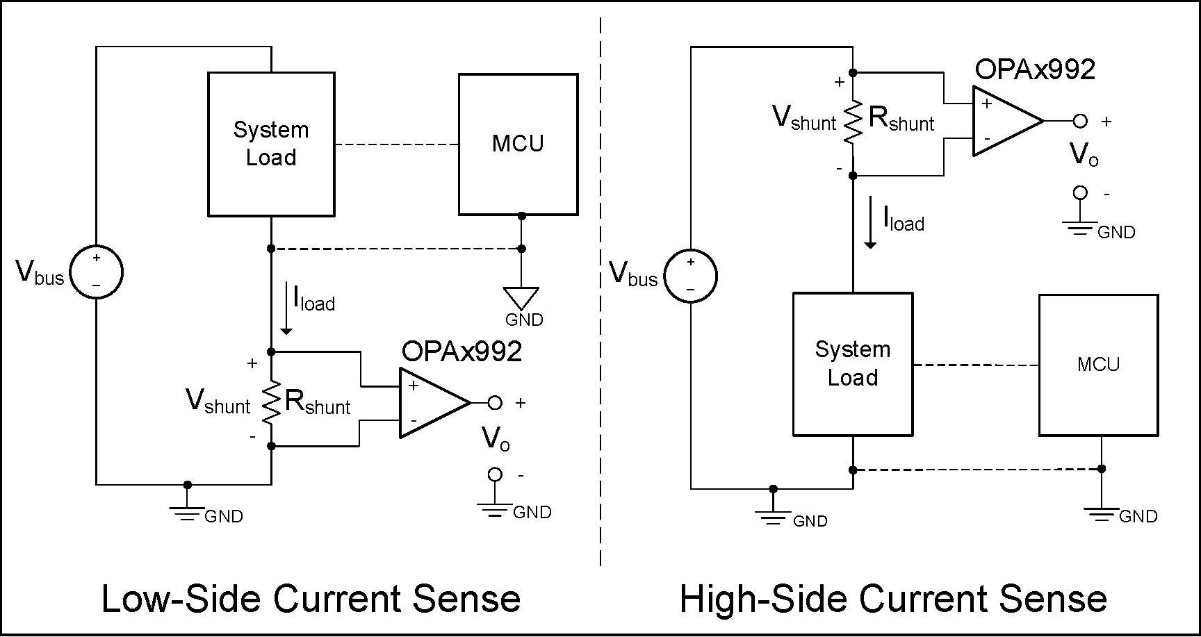
 OPAx992 in Current-Sensing Applications