SBBS002B January 1994 – June 2015 OPT101
PRODUCTION DATA.
- 1 Features
- 2 Applications
- 3 Description
- 4 Revision History
- 5 Pin Configuration and Functions
- 6 Specifications
- 7 Parameter Measurement Information
- 8 Detailed Description
- 9 Application and Implementation
- 10Power-Supply Recommendations
- 11Layout
- 12Device and Documentation Support
- 13Mechanical, Packaging, and Orderable Information
Package Options
Mechanical Data (Package|Pins)
Thermal pad, mechanical data (Package|Pins)
Orderable Information
8 Detailed Description
8.1 Overview
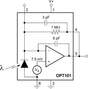
The OPT101 is a large-area photodiode integrated with an optimized operational amplifier that makes the OPT101 a small, easy-to-use, light-to-voltage device. The photodiode has a very large measurement area that collects a significant amount of light, and thus allows for high-sensitivity measurements. The photodiode has a wide spectral response with a maximum peak in the infrared spectrum, and a useable range from 300 nm to 1100 nm. The wide power-supply range of 2.7 V to 36 V makes this device useful in a variety of architectures; from all-analog circuits to data conversion base circuits. The on-chip voltage source keeps the amplifier in a good operating region, even at low light levels.
The OPT101 voltage output is the product of the photodiode current times the feedback resistor, (IDRF), plus a pedestal voltage, VB, of approximately 7.5 mV introduced for single-supply operation. Output is 7.5 mV dc with no light, and increases with increasing illumination. Photodiode current, ID, is proportional to the radiant power, or flux, (in watts) falling on the photodiode. At a wavelength of 650 nm (visible red) the photodiode responsivity, RI, is approximately 0.45 A/W. Responsivity at other wavelengths is shown in Figure 1. The internal feedback resistor is laser trimmed to 1 MΩ. Using this resistor, the output voltage responsivity, RV, is approximately 0.45 V/μW at 650-nm wavelength.
See Figure 2 for the response throughout a wide range of radiant power in microwatts. Figure 3 shows the response throughout a wide range of irradiance in watts per square meter.
8.2 Functional Block Diagram
8.3 Feature Description
8.3.1 Dark Performance
The dark errors in the Electrical Characteristics table include all sources. The dominant source of dark output voltage is the pedestal voltage applied to the noninverting input of the op amp. This voltage is introduced to provide linear operation in the absence of light falling on the photodiode. Photodiode dark current is approximately 2.5 pA, and contributes virtually no offset error at room temperature. The bias current of the op amp summing junction (negative input) is approximately 165 pA. The dark current is subtracted from the amplifier bias current, and this residual current flows through the feedback resistor creating an offset. The effects of temperature on this difference current are seen in Figure 10. The dark output voltage is trimmed to zero with the optional circuit shown in Figure 17. Use a low-impedance offset driver (op amp) to drive pin 8 (Common) because this node has signal-dependent currents.
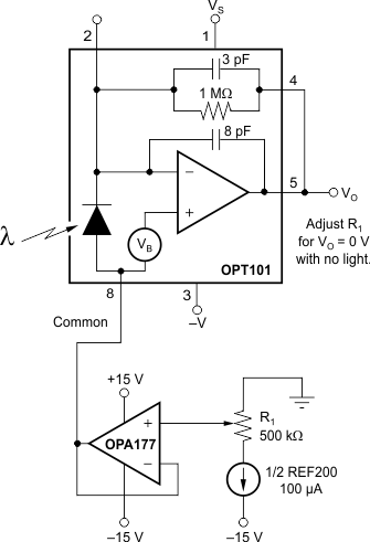 Figure 17. Dark Error (Offset) Adjustment Circuit
8.3.2 Feedback Network and Dynamic Response
The OPT101 features a feedback network for optimal dynamic response. The dynamic response of the OPT101 is dominated by the feedback network and op amp combination. Using the internal 1-MΩ resistor, the dynamic response of the photodiode and op amp combination can be modeled as a simple RC circuit with a –3-dB cutoff frequency of approximately 14 kHz. The R and C values are 1 MΩ and 11 pF, respectively. To improve the frequency response, use external resistors with less than 3-pF parasitic capacitance. An external 1-MΩ resistor used in the configuration shown in Figure 19 creates a 23-kHz bandwidth with the same 106 V/A dc transimpedance gain. This increased bandwidth yields a rise time of approximately 15 μs (10% to 90%). Dynamic response is not limited by op amp slew rate, as demonstrated in Figure 13 and Figure 14, showing virtually identical large-signal and small-signal response.
Dynamic response varies with feedback network value, as shown in Figure 4. Rise time (10% to 90%) varies as a function of the –3-dB bandwidth produced by the feedback network value shown in Equation 1:
where
- tr is the rise time (10% to 90%)
- fC is the –3dB bandwidth
8.3.2.1 Changing Responsivity
To set a different voltage responsivity, connect an external resistor, REXT. To increase the responsivity, place this resistor in series with the internal 1-MΩ resistor (Figure 18), or replace the internal resistor with an external resistor by not connecting pin 4 (Figure 19). The second configuration also reduces the circuit gain below 106 V/A when using external resistors that are less than 1 MΩ.
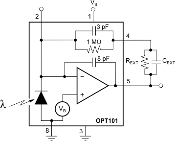 Figure 18. Changing Responsivity with External Resistor in Series with Internal Resistor
Table 1. Responsivity and Bandwidth for Figure 18
| REXT
(MΩ) |
CEXT
(pF) |
DC Gain (× 106V/A) |
Bandwidth (kHz) |
|---|---|---|---|
| 1 | 50 | 2 | 8 |
| 2 | 25 | 3 | 6 |
| 5 | 10 | 6 | 2.5 |
| 10 | 5 | 11 | 1.3 |
| 50 | — | 51 | 0.33 |
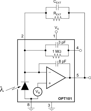 Figure 19. Changing Responsivity with External Resistor Only (Internal Resistor Disabled)
Table 2. Responsivity and Bandwidth for Figure 19
| REXT
(MΩ) |
CEXT
(pF) |
DC Gain (× 106V/A) |
Bandwidth (kHz) |
|---|---|---|---|
| 0.05(1) | 56 | 0.05 | 58 |
| 0.1(1) | 33 | 0.1 | 44 |
| 1 | — | 1 | 23 |
| 2 | — | 2 | 9.4 |
| 5 | — | 5 | 3.6 |
| 10 | — | 10 | 1.8 |
| 50 | — | 50 | 0.34 |
Applications using a feedback resistor significantly larger than the internal 1-MΩ resistor require special consideration. Input bias current of the op amp and dark current of the photodiode increase significantly at higher temperatures. This increase combined with the higher gain (RF > 1 MΩ) can cause the op amp output to be driven to ground at high temperatures. If this problem occurs, use a positive bias voltage applied to pin 8 to make sure that the op amp output remains in the linear operating region when the photodiode is not exposed to light. Alternatively, use a dual power supply. The output may be negative when sensing dark conditions. Use the information discussed in the Dark Performance section and Figure 10 to analyze the desired configuration.
8.3.3 Noise Performance
Noise performance of the OPT101 is determined by the op amp characteristics, feedback network, photodiode capacitance, and signal level. Figure 11 shows how the noise varies with RF and measured bandwidth (0.1 Hz to the indicated frequency), when the output voltage minus the voltage on pin 3 (–V) is greater than approximately 50 mV. Below this level, the output stage is powered down, and the effective bandwidth is decreased. This decreased bandwidth reduces the noise to approximately 1/3 the nominal noise value of 300 μVrms, or 100 μVrms. This decreased bandwidth enables a low-level signal to be resolved.
To reduce noise and improve the signal-to-noise ratio, filter the output with a cutoff frequency equal to the signal bandwidth. In addition, output noise increases in proportion to the square root of the feedback resistance, while responsivity increases linearly with feedback resistance. To improve the signal-to-noise ratio performance, use large feedback resistance, if decreased bandwidth is acceptable to the application.
The noise performance of the photodetector is sometimes characterized by noise effective power (NEP), the radiant power that produces an output signal equal to the noise level. NEP has the units of radiant power (watts), or W/√Hz to convey spectral information about the noise. Figure 12 illustrates the NEP for the OPT101.
8.3.4 Linearity Performance
The photodiode is operated in the photoconductive mode so the current output of the photodiode is very linear with radiant power throughout a wide range. Nonlinearity remains less than approximately 0.05% for photodiode currents less than 100-μA. The photodiode is able to produce output currents of 1 mA or greater with high radiant power, but nonlinearity increases to several percent in this region.
This very linear performance at high radiant power assumes that the full photodiode area is uniformly illuminated. If the light source is focused to a small area of the photodiode, nonlinearity occurs at lower radiant power.
8.3.5 Capacitive Load Drive
The OPT101 is capable of driving load capacitances of 10 nF without instability. However, dynamic performance with capacitive loads may improve by applying a negative bias voltage to pin 3 (–V, shown in Figure 20). This negative power-supply voltage allows the output to go negative in response to the reactive effect of a capacitive load. An internal JFET connected between pin 5 (output) and pin 3 (–V) allows the output to sink current. This current sink capability is also useful when driving the capacitive inputs of some analog-to-digital converters that require the signal source to sink currents up to approximately 100 μA. The benefits of this current sink are shown in Figure 15 and Figure 16. These figures compare operation with pin 3 (–V) grounded and connected to –15 V.
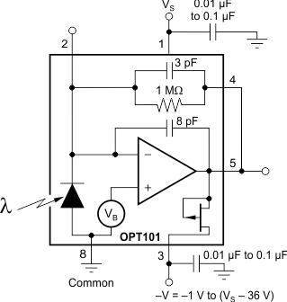 Figure 20. Bipolar Power-Supply Circuit Connections
Because of the architecture of this output stage current sink, there is a slight increase in operating current when there is a voltage between pin 3 (–V) and the output. Depending on the magnitude of this voltage, the quiescent current increases by approximately 100 μA, as shown in Figure 8.
8.4 Device Functional Modes
The OPT101 has a single functional mode and is operational when the power-supply voltage is greater than 2.7 V. The maximum power supply voltage for the OPT101 is 36 V.