SBBS002B January 1994 – June 2015 OPT101
PRODUCTION DATA.
- 1 Features
- 2 Applications
- 3 Description
- 4 Revision History
- 5 Pin Configuration and Functions
- 6 Specifications
- 7 Parameter Measurement Information
- 8 Detailed Description
- 9 Application and Implementation
- 10Power-Supply Recommendations
- 11Layout
- 12Device and Documentation Support
- 13Mechanical, Packaging, and Orderable Information
Package Options
Mechanical Data (Package|Pins)
Thermal pad, mechanical data (Package|Pins)
Orderable Information
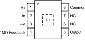
5 Pin Configuration and Functions
DTL and NTC Packages
8-pin SOP and 8-pin PDIP
Top View

1. Photodiode location.
Pin Functions
| PIN | I/O | DESCRIPTION | |
|---|---|---|---|
| NO. | NAME | ||
| 1 | VS | Power | Power supply of device. Apply 2.7 V to 36 V relative to –V pin. |
| 2 | –In | Input | Negative input of op amp and the cathode of the photodiode. Either do not connect, or apply additional op amp feedback. |
| 3 | –V | Power | Most negative power supply. Connect to ground or a negative voltage that meets the recommended operating conditions. |
| 4 | 1MΩ Feedback | Input | Connection to internal feedback network. Typically connect to Output, pin 5. |
| 5 | Output | Output | Output of device. |
| 6 | NC | — | Do not connect |
| 7 | NC | — | Do not connect |
| 8 | Common | Input | Anode of the photodiode. Typically, connect to ground. |