SBAS704B June 2015 – October 2015 OPT8241
PRODUCTION DATA.
- 1 Features
- 2 Applications
- 3 Description
- 4 Revision History
- 5 Pin Configuration and Functions
- 6 Specifications
- 7 Detailed Description
- 8 Application and Implementation
- 9 Power Supply Recommendations
- 10Layout
- 11Device and Documentation Support
- 12Mechanical, Packaging, and Orderable Information
Package Options
Mechanical Data (Package|Pins)
- NBN|78
Thermal pad, mechanical data (Package|Pins)
Orderable Information
7 Detailed Description
7.1 Overview
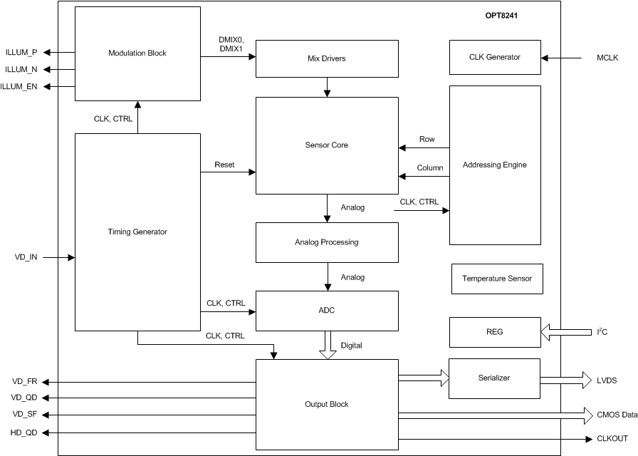
The OPT8241 is a high-performance quarter video graphics array (QVGA) resolution, 3D sensor device that senses depth information based on the time of flight (ToF) technique. The OPT8241 has a CMOS image sensor core with an integrated analog-to-digital converter (ADC), an addressing engine for the sensor core, an low-voltage differential signaling (LVDS) serializer, and an I2C slave device. The device supports configurable timings to optimize power and performance.
The OPT8241 includes the following blocks:
- Timing generator (TG)
- Sensor core
- Addressing engine
- ADC and overload detection
- Modulation block
- Output block
- Temperature sensor
- I2C control interface
7.2 Functional Block Diagram

7.3 Feature Description
7.3.1 Output Block
The output block provides the output data, clock, and frame boundary signals. The positions of the following frame boundary marker signals are programmable. Table 1 lists signals that can be used by the host processor to reconstruct the frame.
Table 1. Output Frame Marker Signals
| SIGNAL | TYPE | DESCRIPTION |
|---|---|---|
| VD_FR | Output | Frame sync |
| VD_SF | Output | Sub-frame sync |
| VD_QD | Output | Quad sync |
| HD_QD | Output | Row sync |
7.3.1.1 Serializer and LVDS Output Interface
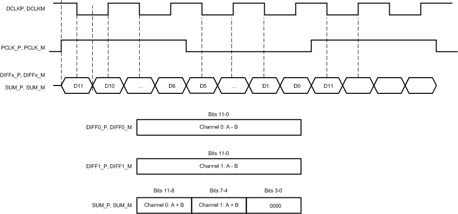
The sensor has an option for a serial LVDS interface. The digitized data from the ADCs are serialized and sent on three LVDS data pairs and one LVDS pixel clock pair. The DIFF0, DIFF1 pairs provide the differential data
(A-B). The differential data for each pixel is 12 bits long. The pixel clock pair is 0 for the first six data bits and 1 for the next six data bits. The pixel clock can be used by the external host to identify the boundary of the 12-bit data for each pixel. The LVDS waveforms are shown in Figure 6.
 Figure 6. LVDS Output Waveforms
7.3.1.2 Parallel CMOS Output Interface
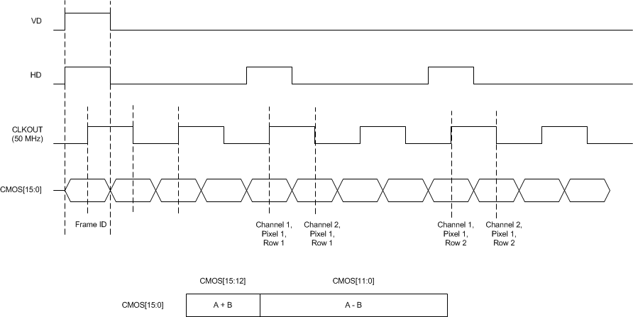
The sensor has options for both serial and parallel data output interfaces. The output data on the parallel CMOS interface toggles on both edges of the clock (DDR rate) with the output clock frequency being equal to the system clock frequency. The CMOS parallel data waveforms are shown in Figure 7.
 Figure 7. CMOS Output waveforms
Following the VD start, the first sample set is a frame ID that denotes the quadrant (quad) number. The frame ID format is given in Table 2.
Table 2. Frame ID Word Format
| 15 | 14 | 13 | 12 | 11 | 10 | 9 | 8 | 7 | 6 | 5 | 4 | 3 | 2 | 1 | 0 |
|---|---|---|---|---|---|---|---|---|---|---|---|---|---|---|---|
| 0 | 1 | 0 | 1 | 0 | 1 | 0 | 1 | SF[3:0] | Q[3:0] | ||||||
Note that Q[3:0] is the quad number and SF[3:0] denotes the sub-frame number.
7.3.2 Temperature Sensor
The on-die temperature sensor can measure temperatures in the range of –25°C to 125°C. The temperature is updated every 3 ms. The temperature value is stored in a register that can be read through the I2C interface.
7.4 Device Functional Modes
All OPT8241 control commands are directed through the OPT9221 time-of-flight controller. For more details on the functional modes of the chipset, see the OPT9221 datasheet.
7.5 Programming
The device registers are programmed by the OPT9221 time-of-flight controller. Therefore, in a typical system, the I2C interface is connected to the OPT9221 sensor control I2C bus; see the OPT9221 datasheet for more details.