SCPS144C May 2006 – May 2015 P82B96
PRODUCTION DATA.
- 1 Features
- 2 Applications
- 3 Description
- 4 Revision History
- 5 Description (continued)
- 6 Pin Configuration and Functions
-
7 Specifications
- 7.1 Absolute Maximum Ratings
- 7.2 ESD Ratings
- 7.3 Recommended Operating Conditions
- 7.4 Thermal Information
- 7.5 Electrical Characteristics: VCC = 2.3 V to 2.7 V
- 7.6 Electrical Characteristics: VCC = 3 V to 3.6 V
- 7.7 Electrical Characteristics: VCC = 4.5 V to 5.5 V
- 7.8 Electrical Characteristics: VCC = 15 V
- 7.9 Switching Characteristics
- 7.10 Typical Characteristics
- 8 Parameter Measurement Information
- 9 Detailed Description
- 10Application and Implementation
- 11Power Supply Recommendations
- 12Layout
- 13Device and Documentation Support
- 14Mechanical, Packaging, and Orderable Information
Package Options
Mechanical Data (Package|Pins)
Thermal pad, mechanical data (Package|Pins)
Orderable Information
1 Features
- Operating Power-Supply Voltage Range of 2 V to 15 V
- Can Interface Between I2C Buses Operating at Different Logic Levels (2 V to 15 V)
- Longer Cables by allowing bus capacitance of 400 pF on Main Side (Sx/Sy) and 4000 pF on Transmission Side (Tx/Ty)
- Outputs on the Transmission Side (Tx/Ty) Have High Current Sink Capability for Driving Low-Impedance or High-Capacitive Buses
- Interface With Optoelectrical Isolators and Similar Devices That Need Unidirectional Input and Output Signal Paths by Splitting I2C Bus Signals Into Pairs of Forward (Tx/Ty) and Reverse (Rx/Ry) Signals
- 400-kHz Fast I2C Bus Operation Over at Least 20 Meters of Wire
- Latch-Up Performance Exceeds 100 mA Per JESD 78, Class II
- ESD Protection Exceeds JESD 22
2 Applications
- HDMI DDC
- Long I2C Communication
- Galvanic I2C Isolation
- Industrial Communications
3 Description
The P82B96 device is a bus buffer that supports bidirectional data transfer between an I2C bus and a range of other bus configurations with different voltage and current levels.
One of the advantages of the P82B96 is that it supports longer cables/traces and allows for more devices per I2C bus because it can isolate bus capacitance such that the total loading (devices and trace lengths) of the new bus or remote I2C nodes are not apparent to other I2C buses (or nodes). The restrictions on the number of I2C devices in a system due to capacitance, or the physical separation between them, are greatly improved.
The device is able to provide galvanic isolation (optocoupling) or use balanced transmission lines (twisted pairs), because separate directional Tx and Rx signals are provided. The Tx and Rx signals may be connected directly (without causing bus latching), to provide an bidirectional signal line with I2C properties (open-drain driver). Likewise, the Ty and Ry signals may also be connected together to provide an bidirectional signal line with I2C properties (open-drain driver). This allows for a simple communication design, saving design time and costs.
Device Information(1)
| PART NUMBER | PACKAGE | BODY SIZE (NOM) |
|---|---|---|
| P82B96 | SOIC (8) | 4.90 mm × 3.91 mm |
| VSSOP (8) | 3.00 mm × 3.00 mm | |
| PDIP (8) | 9.81 mm × 6.35 mm | |
| TSSOP (8) | 3.00 mm × 4.40 mm |
- For all available packages, see the orderable addendum at the end of the data sheet.
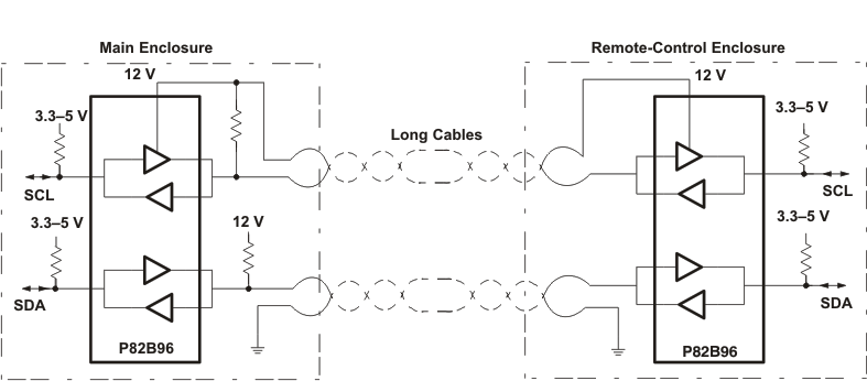
Long-Distance I2C Communications
