SCPS144C May 2006 – May 2015 P82B96
PRODUCTION DATA.
- 1 Features
- 2 Applications
- 3 Description
- 4 Revision History
- 5 Description (continued)
- 6 Pin Configuration and Functions
-
7 Specifications
- 7.1 Absolute Maximum Ratings
- 7.2 ESD Ratings
- 7.3 Recommended Operating Conditions
- 7.4 Thermal Information
- 7.5 Electrical Characteristics: VCC = 2.3 V to 2.7 V
- 7.6 Electrical Characteristics: VCC = 3 V to 3.6 V
- 7.7 Electrical Characteristics: VCC = 4.5 V to 5.5 V
- 7.8 Electrical Characteristics: VCC = 15 V
- 7.9 Switching Characteristics
- 7.10 Typical Characteristics
- 8 Parameter Measurement Information
- 9 Detailed Description
- 10Application and Implementation
- 11Power Supply Recommendations
- 12Layout
- 13Device and Documentation Support
- 14Mechanical, Packaging, and Orderable Information
Package Options
Mechanical Data (Package|Pins)
Thermal pad, mechanical data (Package|Pins)
Orderable Information
12 Layout
12.1 Layout Guidelines
The recommended decoupling capacitors should be placed as close to the VCC pin of the P82B96 as possible.
12.2 Layout Example
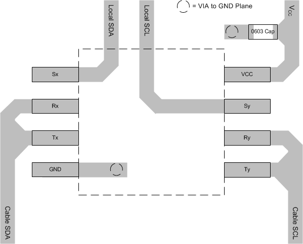
Figure 16 is an example layout for the typical application seen in the Long-Distance I2C section, using the DGK package.
 Figure 16. Layout Example