SCPS144C May   2006  – May 2015 P82B96

PRODUCTION DATA.  

  1. Features
  2. Applications
  3. Description
  4. Revision History
  5. Description (continued)
  6. Pin Configuration and Functions
  7. Specifications
    1. 7.1  Absolute Maximum Ratings
    2. 7.2  ESD Ratings
    3. 7.3  Recommended Operating Conditions
    4. 7.4  Thermal Information
    5. 7.5  Electrical Characteristics: VCC = 2.3 V to 2.7 V
    6. 7.6  Electrical Characteristics: VCC = 3 V to 3.6 V
    7. 7.7  Electrical Characteristics: VCC = 4.5 V to 5.5 V
    8. 7.8  Electrical Characteristics: VCC = 15 V
    9. 7.9  Switching Characteristics
    10. 7.10 Typical Characteristics
  8. Parameter Measurement Information
  9. Detailed Description
    1. 9.1 Overview
    2. 9.2 Functional Block Diagram
    3. 9.3 Feature Description
      1. 9.3.1 Sx and Sy
      2. 9.3.2 Tx and Ty
      3. 9.3.3 Long Cable Length
    4. 9.4 Device Functional Modes
  10. 10Application and Implementation
    1. 10.1 Application Information
      1. 10.1.1 Calculating System Delays and Bus-Clock Frequency for Fast Mode System
        1. 10.1.1.1 Sample Calculations
    2. 10.2 Typical Applications
      1. 10.2.1 Driving Ribbon or Flat Telephone Cables
        1. 10.2.1.1 Design Requirements
        2. 10.2.1.2 Detailed Design Procedure
        3. 10.2.1.3 Application Curve
      2. 10.2.2 Galvanic Isolation
      3. 10.2.3 Long-Distance I2C
      4. 10.2.4 Extend I2C/DDC Bus With Short-Circuit Protection
      5. 10.2.5 Voltage Translation
  11. 11Power Supply Recommendations
  12. 12Layout
    1. 12.1 Layout Guidelines
    2. 12.2 Layout Example
  13. 13Device and Documentation Support
    1. 13.1 Community Resources
    2. 13.2 Trademarks
    3. 13.3 Electrostatic Discharge Caution
    4. 13.4 Glossary
  14. 14Mechanical, Packaging, and Orderable Information

Package Options

Mechanical Data (Package|Pins)
Thermal pad, mechanical data (Package|Pins)
Orderable Information

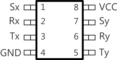
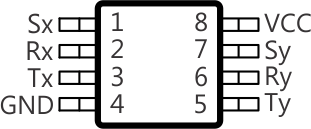
6 Pin Configuration and Functions

P Package
8-Pin PDIP
(Top View)
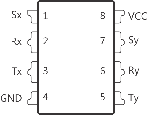
P82B96 po_ppack_cps144.gif
PW Package
8-Pin TSSOP
(Top View)
P82B96 po_pwpack_cps144.gif
D Package
8-Pin SOIC
(Top View)
P82B96 po_dpack_cps144.gif
DGK Package
8-Pin VSSOP
(Top View)
P82B96 po_dgkpack_cps144.gif

Pin Functions

PIN I/O DESCRIPTION
NO. NAME
1 Sx I/O Serial data bus or SDA. Connect to VCC of I2C master through a pullup resistor.
2 Rx I Receive signal. Connect to VCC of P82B96 through a pullup resistor.
3 Tx O Transmit signal. Connect to VCC of P82B96 through a pullup resistor.
4 GND Ground
5 Ty O Transmit signal. Connect to VCC of P82B96 through a pullup resistor.
6 Ry I Receive signal. Connect to VCC of P82B96 through a pullup resistor.
7 Sy I/O Serial clock bus or SCL. Connect to VCC of I2C master through a pullup resistor.
8 VCC I Supply voltage