SCPS129K August 2005 – March 2021 PCA9535
PRODUCTION DATA
- 1 Features
- 2 Description
- 3 Revision History
- 4 Description Continued
- 5 Pin Configuration and Functions
- 6 Specifications
- 7 Parameter Measurement Information
- 8 Detailed Description
- 9 Application Information Disclaimer
- 10Power Supply Recommendations
- 11Device and Documentation Support
- 12Mechanical, Packaging, and Orderable Information
5 Pin Configuration and Functions
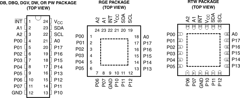
Table 5-1 Pin Functions
| PIN | DESCRIPTION | ||
|---|---|---|---|
| NAME | SOIC (D), SSOP (DB), QSOP (DBQ), TSSOP (PW), AND TVSOP (DGV) |
QFN (RGE AND RTW) |
|
| INT | 1 | 22 | Interrupt output. Connect to VCC through a pullup resistor. |
| A1 | 2 | 23 | Address input. Connect directly to VCC or ground. |
| A2 | 3 | 24 | Address input. Connect directly to VCC or ground. |
| P00 | 4 | 1 | P-port input/output. Push-pull design structure. |
| P01 | 5 | 2 | P-port input/output. Push-pull design structure. |
| P02 | 6 | 3 | P-port input/output. Push-pull design structure. |
| P03 | 7 | 4 | P-port input/output. Push-pull design structure. |
| P04 | 8 | 5 | P-port input/output. Push-pull design structure. |
| P05 | 9 | 6 | P-port input/output. Push-pull design structure. |
| P06 | 10 | 7 | P-port input/output. Push-pull design structure. |
| P07 | 11 | 8 | P-port input/output. Push-pull design structure. |
| GND | 12 | 9 | Ground |
| P10 | 13 | 10 | P-port input/output. Push-pull design structure. |
| P11 | 14 | 11 | P-port input/output. Push-pull design structure. |
| P12 | 15 | 12 | P-port input/output. Push-pull design structure. |
| P13 | 16 | 13 | P-port input/output. Push-pull design structure. |
| P14 | 17 | 14 | P-port input/output. Push-pull design structure. |
| P15 | 18 | 15 | P-port input/output. Push-pull design structure. |
| P16 | 19 | 16 | P-port input/output. Push-pull design structure. |
| P17 | 20 | 17 | P-port input/output. Push-pull design structure. |
| A0 | 21 | 18 | Address input. Connect directly to VCC or ground. |
| SCL | 22 | 19 | Serial clock bus. Connect to VCC through a pullup resistor. |
| SDA | 23 | 20 | Serial data bus. Connect to VCC through a pullup resistor. |
| VCC | 24 | 21 | Supply voltage |