SCPS146G October   2005  – March 2021 PCA9544A

PRODUCTION DATA  

  1. Features
  2. Applications
  3. Description
  4. Revision History
  5. Pin Configuration and Functions
  6. Specifications
    1. 6.1 Absolute Maximum Ratings
    2. 6.2 ESD Ratings
    3. 6.3 Recommended Operating Conditions
    4. 6.4 Thermal Information
    5. 6.5 Electrical Characteristics
    6. 6.6 I2C Interface Timing Requirements
    7. 6.7 Switching Characteristics
    8. 6.8 Interrupt Timing Requirements
  7. Parameter Measurement Information
  8. Detailed Description
    1. 8.1 Overview
    2. 8.2 Functional Block Diagram
    3. 8.3 Feature Description
    4. 8.4 Device Functional Modes
      1. 8.4.1 Power-On Reset
    5. 8.5 Programming
      1. 8.5.1 I2C Interface
    6. 8.6 Register Map
      1. 8.6.1 Control Register
        1. 8.6.1.1 Device Address
        2. 8.6.1.2 Control Register Description
        3. 8.6.1.3 Control Register Definition
        4. 8.6.1.4 Interrupt Handling
  9. Application Information Disclaimer
    1. 9.1 Application Information
    2. 9.2 Typical Application
      1. 9.2.1 Design Requirements
      2. 9.2.2 Detailed Design Procedure
      3. 9.2.3 Application Curves
  10. 10Power Supply Recommendations
    1. 10.1 Power-On Reset Requirements
  11. 11Layout
    1. 11.1 Layout Guidelines
    2. 11.2 Layout Example
  12. 12Device and Documentation Support
    1. 12.1 Receiving Notification of Documentation Updates
    2. 12.2 Support Resources
    3. 12.3 Trademarks
    4. 12.4 Electrostatic Discharge Caution
    5. 12.5 Glossary
  13. 13Mechanical, Packaging, and Orderable Information

Package Options

Mechanical Data (Package|Pins)
Thermal pad, mechanical data (Package|Pins)
Orderable Information

Control Register Description

Following the successful acknowledgment of the slave address, the bus master sends a byte to the PCA9544A, which is stored in the control register. If multiple bytes are received by the PCA9544A, it saves the last byte received. This register can be written and read via the I2C bus.
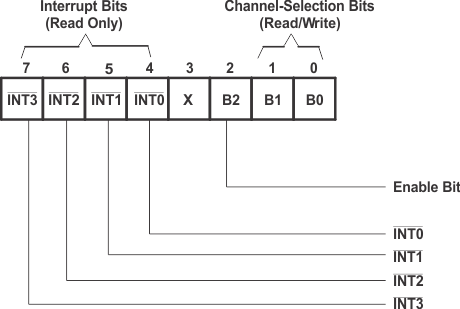
GUID-4F4813C8-C266-4458-822A-AC182A7D37D9-low.gifFigure 8-8 Control Register