SCPS128D July   2006  – March 2021 PCA9554

PRODUCTION DATA  

  1. Features
  2. Description
  3. Revision History
  4. Description (Continued)
  5. Pin Configuration and Functions
  6. Specifications
    1. 6.1 Absolute Maximum Ratings
    2. 6.2 ESD Ratings
    3. 6.3 Recommended Operating Conditions
    4. 6.4 Thermal Information
    5. 6.5 Electrical Characteristics
    6. 6.6 I2C Interface Timing Requirements
    7. 6.7 Switching Characteristics
    8. 6.8 Typical Characteristics
  7. Parameter Measurement Information
  8. Detailed Description
    1. 8.1 Functional Block Diagram
    2. 8.2 Device Functional Modes
      1. 8.2.1 Power-On Reset
      2. 8.2.2 I/O Port
      3. 8.2.3 Interrupt Output ( INT)
        1. 8.2.3.1 Interrupt Errata
          1.        23
          2. 8.2.3.1.1 24
          3. 8.2.3.1.2 25
    3. 8.3 Programming
      1. 8.3.1 I2C Interface
      2. 8.3.2 Register Map
        1. 8.3.2.1 Device Address
        2. 8.3.2.2 Control Register And Command Byte
        3. 8.3.2.3 Register Descriptions
        4. 8.3.2.4 Bus Transactions
          1. 8.3.2.4.1 Writes
          2. 8.3.2.4.2 Reads
  9. Application Information Disclaimer
    1. 9.1 Application Information
      1. 9.1.1 Typical Application
        1. 9.1.1.1 Design Requirements
          1. 9.1.1.1.1 Minimizing ICC When I/Os Control Leds
  10. 10Power Supply Recommendations
    1. 10.1 Power-On Reset Requirements
  11. 11Device and Documentation Support
    1. 11.1 Receiving Notification of Documentation Updates
    2. 11.2 Support Resources
    3. 11.3 Trademarks
    4. 11.4 Electrostatic Discharge Caution
    5. 11.5 Glossary
  12. 12Mechanical, Packaging, and Orderable Information

Package Options

Mechanical Data (Package|Pins)
Thermal pad, mechanical data (Package|Pins)
Orderable Information

Typical Characteristics

TA = 25°C (unless otherwise noted)
GUID-78124F55-48A2-4AFE-A6E3-1DEF0F46EFB5-low.gif
fSCL = 400 kHzI/Os = High or Low Inputs
Figure 6-1 Supply Current (ICC, Operating Mode) vs Temperature (TA) at Four Supply Voltages
GUID-21B61C93-6C5A-4A00-844B-FCECDDA89603-low.gif
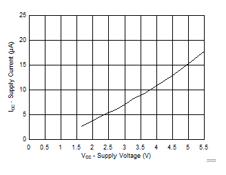
fSCL = 400 kHzI/Os = High or Low InputsTA = 25°C
Figure 6-3 Supply Current (ICC, Operating Mode) vs Supply Voltage (VCC)
GUID-545CC749-DE16-4F11-B216-AA3FB8F80457-low.gif
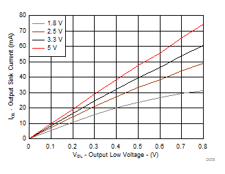
TA = 25°C
Figure 6-5 Sink Current (IOL) vs Output Low Voltage (VOL) for P-Ports at Four Supply Voltages
GUID-DE265D7C-3887-473F-A882-7F167DFBFAFA-low.gif
TA = 25°C
Figure 6-7 Source Current (IOH) vs Output High Voltage (VOH) for P-Ports at Four Supply Voltages
GUID-C86C5111-0D15-4D8D-AEE3-FE760F6CC6E4-low.gif
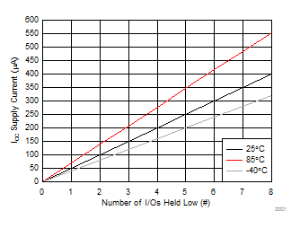
VCC = 5 V
Figure 6-9 Supply Current (ICC) vs Number of I/Os Held Low (#)
GUID-B867BA78-1478-40F5-B881-4722EDFC4892-low.gif
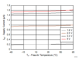
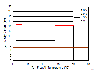
fSCL = 0 kHzI/Os = High Inputs
Figure 6-2 Supply Current (ICC, Standby Mode) vs Temperature (TA) at Four Supply Voltages
GUID-EAA716DC-09B3-41D8-B0B4-D734A557D754-low.gif
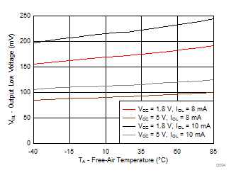
Figure 6-4 Output Low Voltage (VOL) vs Temperature (TA) for P-Port I/Os
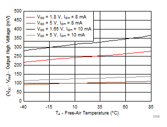
GUID-651F5B6A-8E78-4419-A761-80DEA4DB8129-low.gifFigure 6-6 Output High Voltage (VCC – VOH) vs Temperature (TA) for P-Ports
GUID-785168F7-0DF4-4619-BBA0-826D349433C0-low.gif
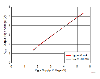
TA = 25°C
Figure 6-8 Output High Voltage (VOH) vs Supply Voltage (VCC) for P-Ports
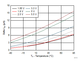
GUID-58A382B0-D2A8-4BEC-8775-670D59C95C0F-low.gifFigure 6-10 Δ ICC vs Temperature for Different VCC (VI = VCC – 0.6 V)