SCPS069H July 2001 – September 2024 PCF8574A
PRODUCTION DATA
- 1
- 1 Features
- 2 Applications
- 3 Description
- 4 Pin Configuration and Functions
- 5 Specifications
- 6 Parameter Measurement Information
- 7 Detailed Description
- 8 Application Information Disclaimer
- 9 Device and Documentation Support
- 10Revision History
- 11Mechanical, Packaging, and Orderable Information
Package Options
Refer to the PDF data sheet for device specific package drawings
Mechanical Data (Package|Pins)
- DGV|20
- DW|16
- N|16
- PW|20
- RGY|20
Thermal pad, mechanical data (Package|Pins)
- DW|16
Orderable Information
7.4 Device Functional Modes
Figure 7-1 and Figure 7-2 show the address and timing diagrams for the write and read modes, respectively.
 Figure 7-1 Write Mode (Output)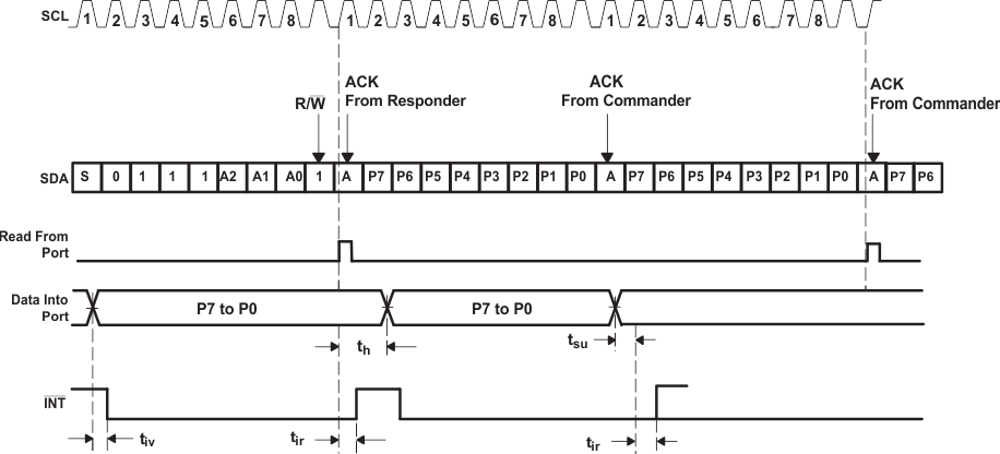
A. A low-to-high transition of SDA while SCL is high is defined as the stop condition (P). The transfer of data can be stopped at any moment bya stop condition. When this occurs, data present at the latest ACK phase is valid (output mode). Input data is lost.
Figure 7-2 Read Mode (Input)